
2 layers148 × 84.5 mm
Panel daisy
ohmtech-rdi/eurorack-blocks
Software to Hardware Prototyping for Eurorack using C++, Max/Gen~ or Faust
259 parts410

 ruproshanjha/Function-Generator-using-TL072-OPAmp
An Analog Function Generator Designed Around the TL072 Dual Op-Amp
FunctionGeneratorPCB is an open-source printed circuit board by ruproshanjha, from the ruproshanjha/Function-Generator-using-TL072-OPAmp repository on GitHub. It is a 2-layer board of 46.5 × 60 mm with 19 parts on 19 nets, routed with 116 tracks and 0 vias.
It is built around the TL072. Its parts include 8 resistors, 3 capacitors, 2 ICs, 2 connectors and 1 switch.
An Analog Function Generator Designed Around the TL072 Dual Op-Amp
This project is a discrete analog function generator built using TL072 operational amplifiers.
The circuit generates multiple periodic waveforms through a combination of op-amp based waveform-generation and signal-conditioning stages. The project was developed from individual circuit stages, simulated in LTSpice, prototyped on a breadboard, and finally designed as a PCB using KiCad.
The project includes the complete design workflow:
Circuit Design → Simulation → Breadboard Prototype → KiCad Schematic → PCB Layout → 3D PCB
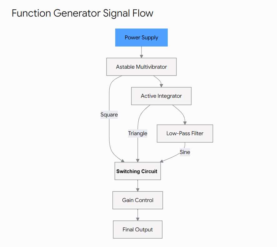
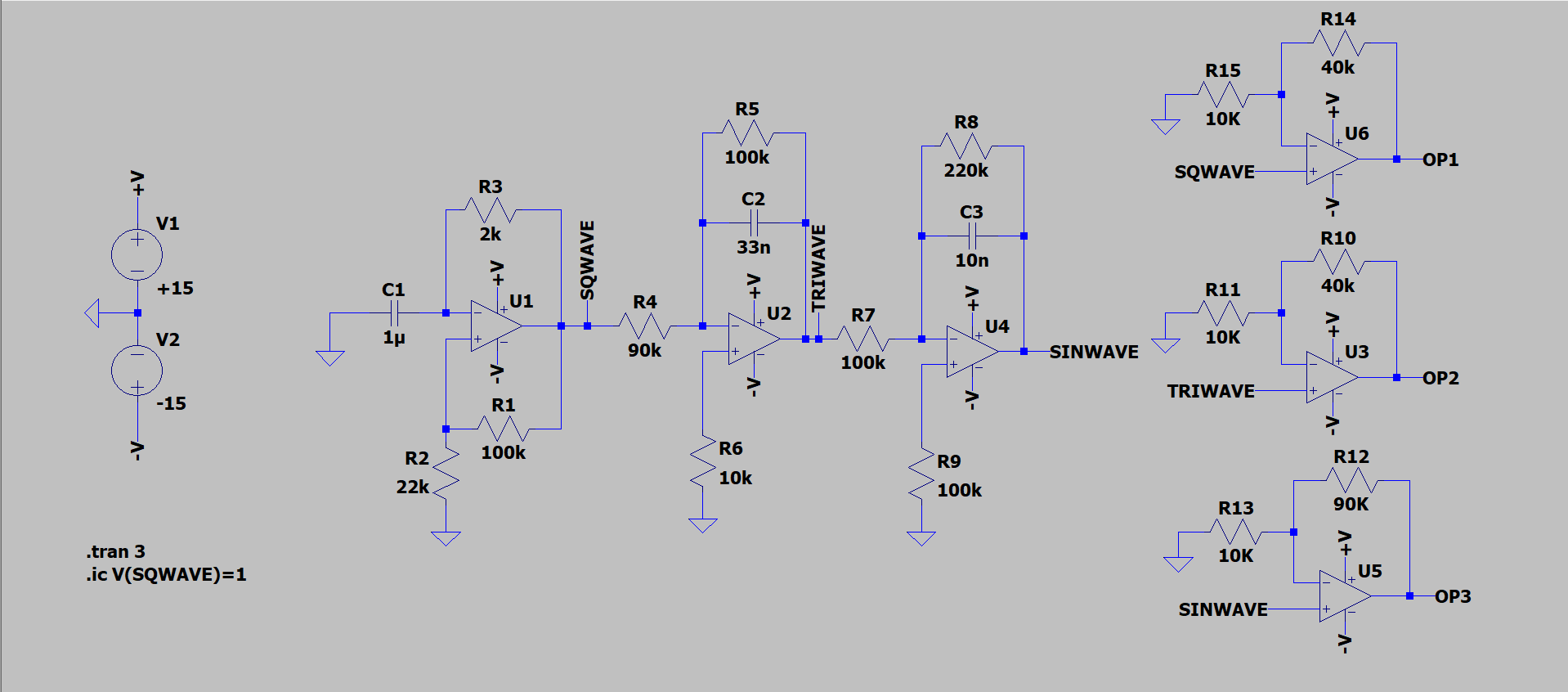
The generator is designed around a waveform-generation chain in which the different stages produce and process the required signals.
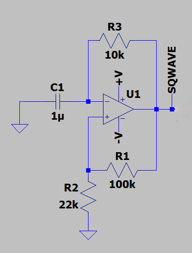
The square-wave stage forms the primary waveform-generation section.
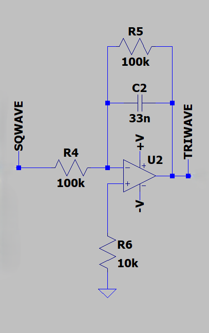
The triangle-wave stage converts the generated waveform into a triangular waveform.
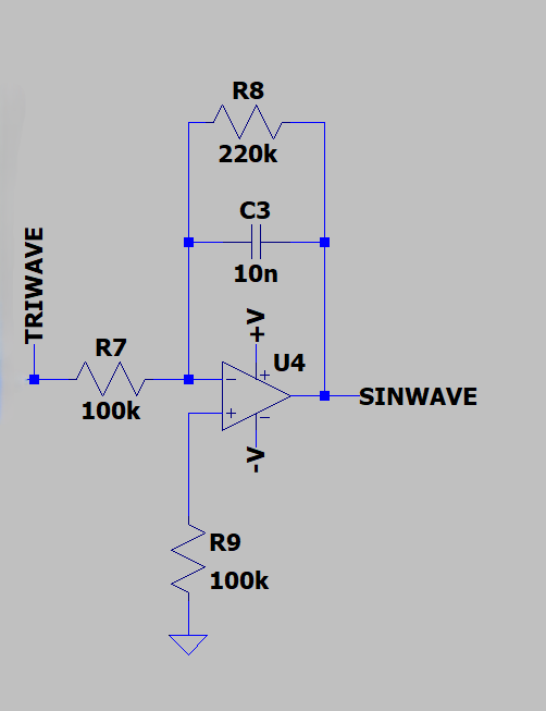
The sine-wave stage processes the generated waveform to obtain a sinusoidal output.
The overall design can be understood as a sequence of functional blocks:
                 ┌─────────────────────┐
                 │   Wave Generation   │
                 │      Stage          │
                 └──────────┬──────────┘
                            │
                            ▼
                 ┌─────────────────────┐
                 │  Waveform Shaping   │
                 │   / Conversion      │
                 └──────────┬──────────┘
                            │
              ┌─────────────┼─────────────┐
              │             │             │
              ▼             ▼             ▼
           Square        Triangle        Sine
              │             │             │
              └─────────────┼─────────────┘
                            │
                            ▼
                 ┌─────────────────────┐
                 │   Gain / Output     │
                 │       Stage         │
                 └──────────┬──────────┘
                            │
                            ▼
OUTPUTA dedicated gain/output circuit is included to condition the generated waveform before it is presented at the output.
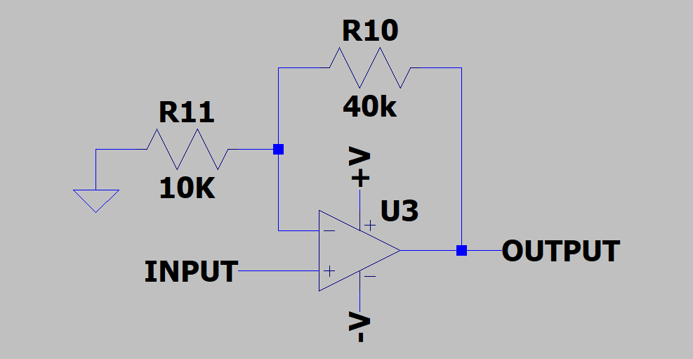
The circuit was simulated using LTSpice before hardware implementation.
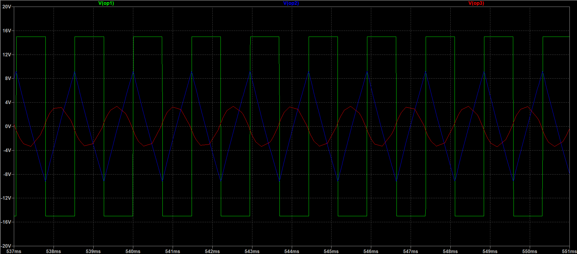
Simulation was used to verify the circuit behavior and waveform generation before moving to physical implementation.
After simulation, the individual stages were implemented and tested on a breadboard.
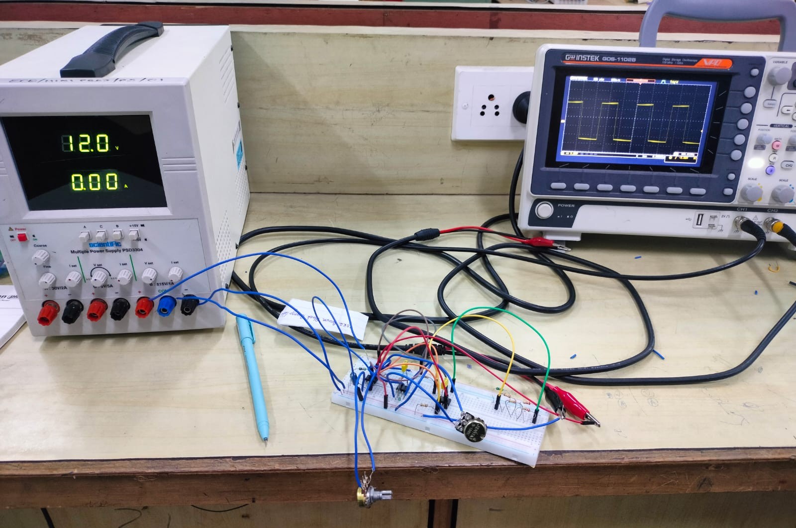
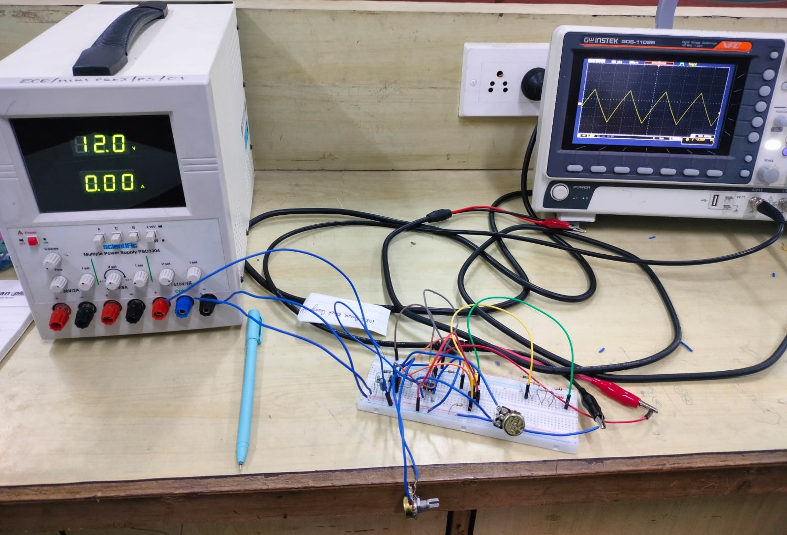
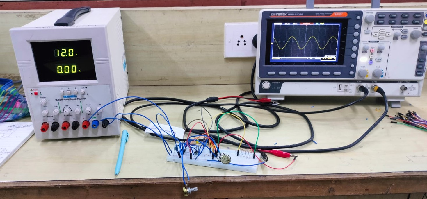
The breadboard implementations were used to validate the practical behavior of the analog circuits before committing to the PCB design.
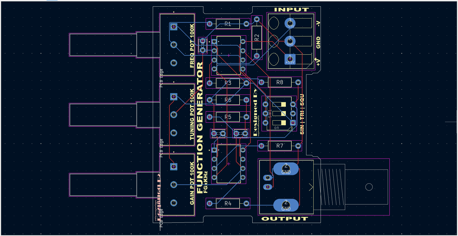
The final hardware design was developed using KiCad.
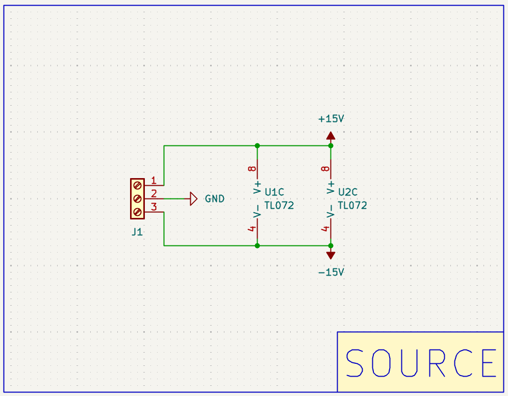
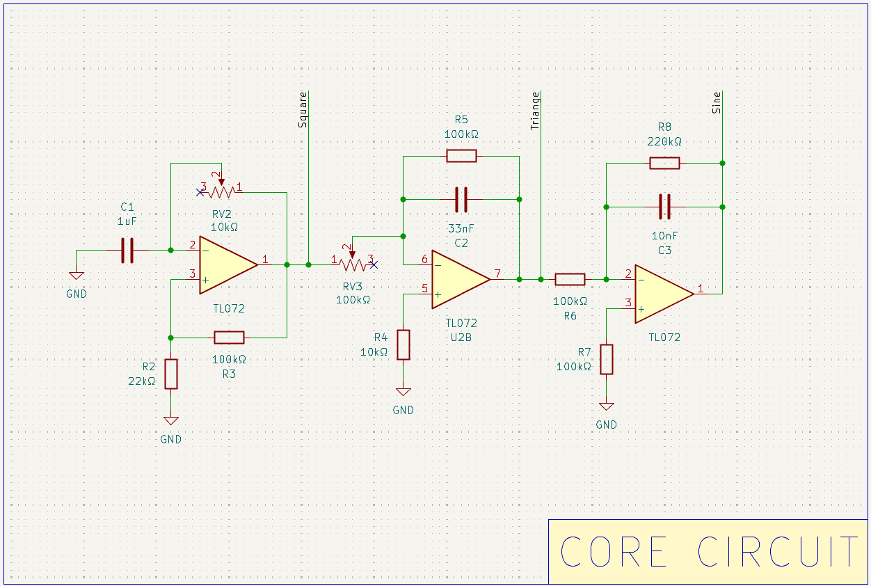
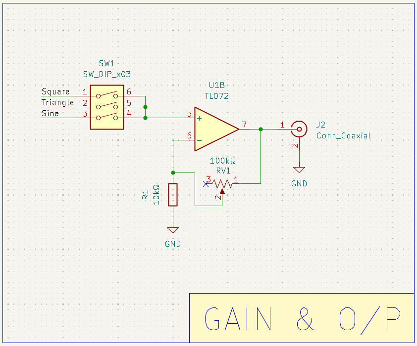
The complete PCB layout was created from the KiCad schematic.
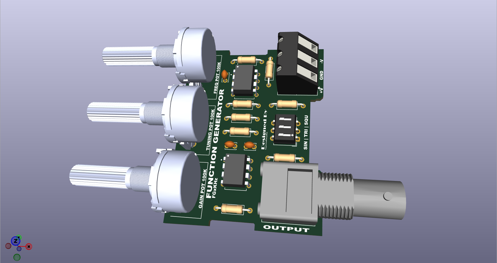
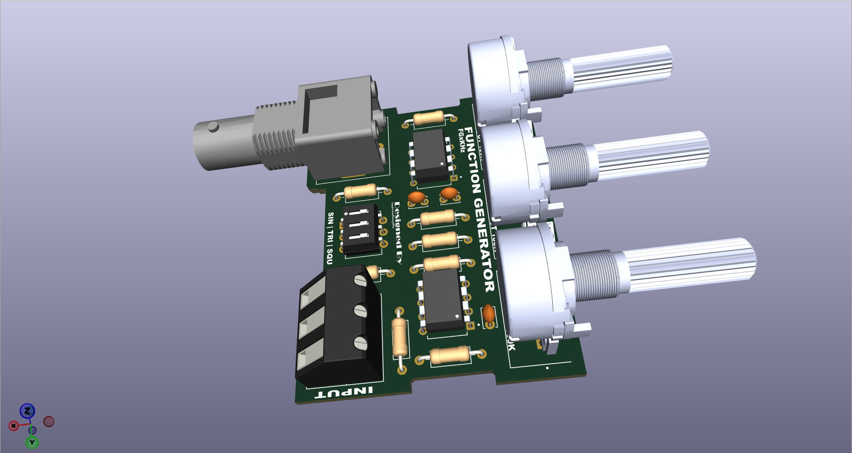
A zero-PCB implementation was also documented as part of the hardware development process.
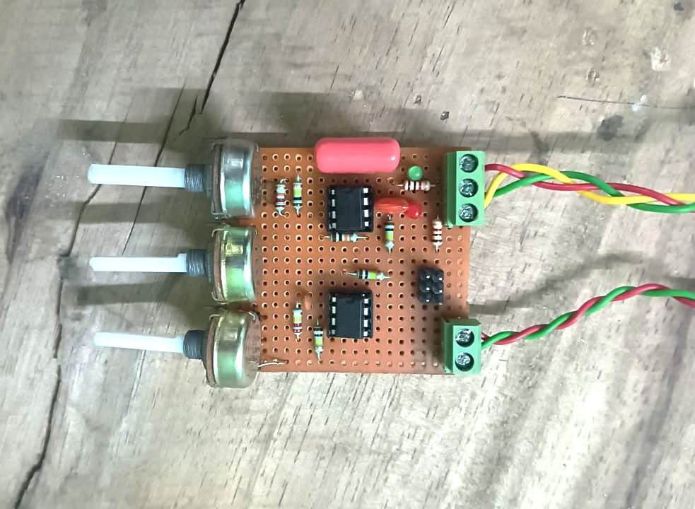
The project also includes analysis of how the oscillator frequency changes with component values.
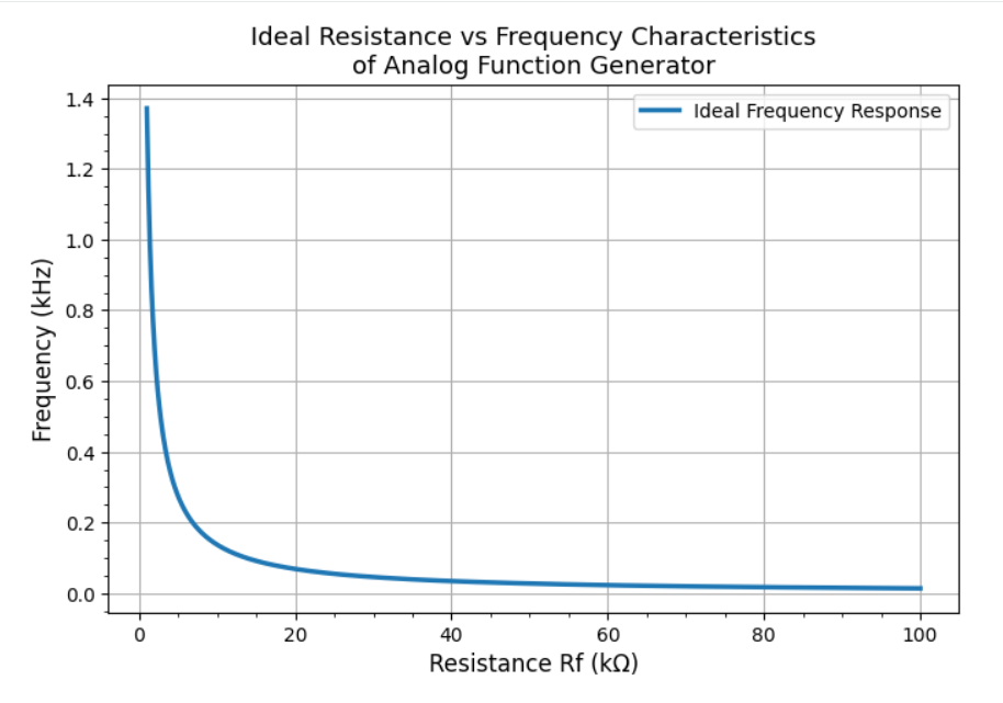
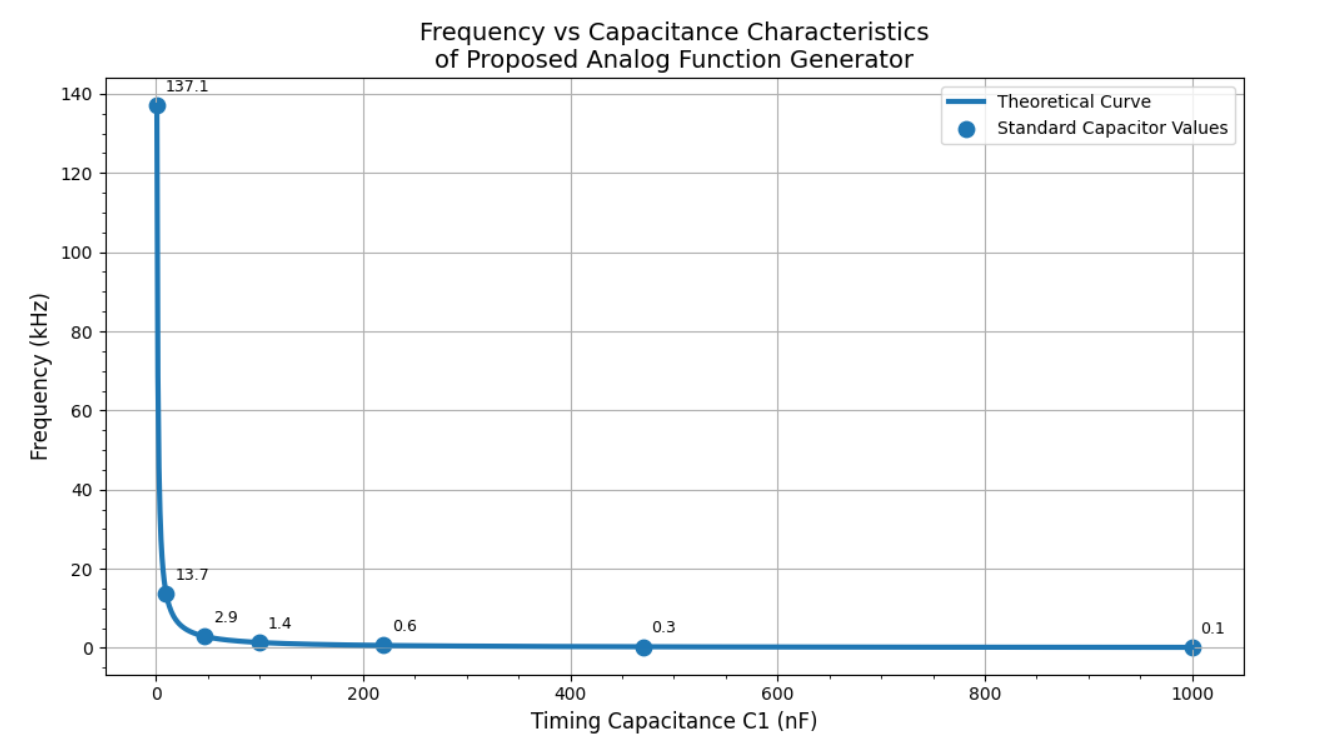
These plots provide a practical reference for understanding the relationship between the timing components and generated frequency.
Function-Generator-using-TL072-OPAmp/
│
├── 3D Models/
│
├── Docs/
│   ├── 00 - Block Diagram.png
│   ├── 01 - Square Wave Circuit.png
│   ├── 02 Triangle Wave Circuit.png
│   ├── 03 - Sine Wave Circuit.png
│   ├── 04 - Gain Circuit.png
│   ├── 05 - LTSpice Schematic.png
│   ├── 06 - LTSpice Simulation Graph.png
│   │
│   ├── 10 - Breadboard Implementation Square.jpeg
│   ├── 11 - Breadboard Implementation Triangle.jpeg
│   ├── 12 - Breadboard Implementation Sine.jpeg
│   │
│   ├── 20 - KiCad Schematic - Source.png
│   ├── 21 - KiCad Schematic - Core Circuit.png
│   ├── 22 - KiCad Schematic - Gain & Output.png
│   ├── 23 - KiCad PCB Layout.png
│   ├── 24 - KiCad 3D View 1.png
│   ├── 25 - KiCad 3D View 2.png
│ │The project followed a complete electronics development workflow:
Individual analog stages were designed for waveform generation and signal conditioning.
The circuits were tested in LTSpice to verify their expected behavior.
The circuits were physically implemented on a breadboard and tested.
The validated design was recreated in KiCad.
The complete circuit was converted into a PCB layout.
The PCB was inspected using KiCad's 3D viewer to verify component placement and overall board design.
The repository contains the main KiCad project files:
| File | Description |
|---|---|
FunctionGeneratorPCB.kicad_pro | KiCad project file |
FunctionGeneratorPCB.kicad_sch | Complete circuit schematic |
FunctionGeneratorPCB.kicad_pcb | PCB layout |
Footprint.pretty/ | Custom footprint library |
3D Models/ | 3D component models |
Docs/ | Design, simulation and hardware documentation |
This project demonstrates several practical analog electronics concepts:
All supporting diagrams, simulation results, prototype photographs, PCB designs and frequency-analysis plots are available in the Docs directory.
Completed — Design, Simulation, Prototyping and PCB Development
The repository contains the design artifacts required to understand and reproduce the project, including the circuit schematics, PCB files, supporting documentation and prototype images.
Rup Roshan Jha
Electronics / Hardware Design Project
See the repository for licensing information.
| Qty | Value | Footprint | References |
|---|---|---|---|
| 4 | 100kΩ | Resistor_THT:R_Axial_DIN0207_L6.3mm_D2.5mm_P10.16mm_Horizontal | R3, R5, R6, R7 |
| 3 | 100kΩ | Footprint:POT_PTN16-A100125K1B1 | RV1, RV2, RV3 |
| 2 | 10kΩ | Resistor_THT:R_Axial_DIN0207_L6.3mm_D2.5mm_P10.16mm_Horizontal | R1, R4 |
| 2 | TL072 | Footprint:TL072 | U1, U2 |
| 1 | 10nF | Capacitor_THT:C_Disc_D3.4mm_W2.1mm_P2.50mm | C3 |
| 1 | 1uF | Capacitor_THT:C_Disc_D3.4mm_W2.1mm_P2.50mm | C1 |
| 1 | 220kΩ | Resistor_THT:R_Axial_DIN0207_L6.3mm_D2.5mm_P10.16mm_Horizontal | R8 |
| 1 | 22kΩ | Resistor_THT:R_Axial_DIN0207_L6.3mm_D2.5mm_P10.16mm_Horizontal | R2 |
| 1 | 33nF | Capacitor_THT:C_Disc_D3.4mm_W2.1mm_P2.50mm | C2 |
| 1 | Conn_Coaxial | Connector_Coaxial:BNC_Amphenol_B6252HB-NPP3G-50_Horizontal | J2 |
| 1 | SW_DIP_x03 | Button_Switch_THT:SW_DIP_SPSTx03_Slide_6.7x9.18mm_W7.62mm_P2.54mm_LowProfile | SW1 |
| 1 | Screw_Terminal_01x03 | TerminalBlock_Altech:Altech_AK300_1x03_P5.00mm_45-Degree | J1 |
ohmtech-rdi/eurorack-blocks
Software to Hardware Prototyping for Eurorack using C++, Max/Gen~ or Faust

ctag-fh-kiel/ctag-tbd
CTAG TBD >>to be determined<< an extendible open source Eurorack sound module

plinkysynth/plinky_public
a public release of the plinky sw and hw


matthewcieplak/super-sixteen
Code and schematics for the Super Sixteen Eurorack sequencer

mzuelch/CATs-Eurosynth
Analog Synth Eurorack Modules

StoneRose35/cortexguitarfx
guitar effects processor implemented on various arm cortex platforms
It measures 46.5 × 60 mm and has 2 copper layers, 1.6 mm thick.
19 parts, built around the TL072. The full list of its parts is on this page, with links to each part's symbol and footprint where PCBKit's library has them.
From the ruproshanjha/Function-Generator-using-TL072-OPAmp repository on GitHub, at the commit this page was made from: the board is FunctionGeneratorPCB.kicad_pcb and its schematic FunctionGeneratorPCB.kicad_sch. PCBKit opens the board in the browser, with nothing to install.
Its repository states no licence, so its author keeps all rights: ask ruproshanjha before reusing the design.