4 layers30.7 × 56.9 mm
ESP32 Clone devkit
futureshocked/KLP3e_ESP32_development_kit
This is the repository for the "ESP32 Devkit clone" project.
36 parts5
 RTX17LEO/ESP-32-DEV-MODULE
The ESP32 Dev Module is a powerful microcontroller with built-in Wi-Fi and Bluetooth, widely used for IoT and embedded applications.
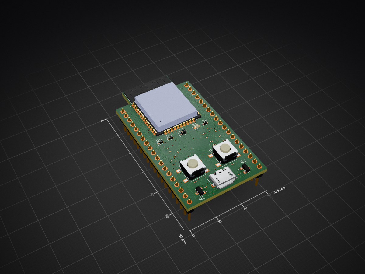
ESP 32 DEV KIT PCB Layout is an open-source printed circuit board by RTX17LEO, from the RTX17LEO/ESP-32-DEV-MODULE repository on GitHub. It is a 4-layer board of 30.5 × 56.8 mm with 34 parts on 70 nets, routed with 856 tracks and 63 vias.
It is built around the CP2102N-A01-GQFN28R, ESP32-WROOM-32 and AMS1117-3.3, with the MMSS8050-H-TP among its other parts. Its parts include 10 resistors, 9 capacitors, 5 diodes, 3 connectors and 2 ICs. It belongs with the ESP32 boards of this library.


ESP32 Dev Board Project
The ESP32 Dev Module is a powerful microcontroller with built-in Wi-Fi and Bluetooth, widely used for IoT and embedded applications.
This project includes the schematic and PCB design of an ESP32 Dev Module created using KiCad.
The schematic defines connections for power, EN pin, and basic components like resistors and capacitors.
A 2-layer PCB is designed with proper routing and clearance rules followed.
KiCad is used for schematic capture, footprint assignment, and PCB layout, and Gerber files are generated for manufacturing.
| Qty | Value | Footprint | References |
|---|---|---|---|
| 3 | 0.1uF/50V/(10%) | Capacitor_SMD:C_01005_0402Metric | C9, C19, C22 |
| 3 | 10k(5%) | Resistor_SMD:R_01005_0402Metric | R11, R21, R22 |
| 3 | 22uF/10v(20%) | Capacitor_SMD:C_0201_0603Metric | C1, C3, C21 |
| 3 | D_TVS | Diode_SMD:D_SOD-523 | D3, D4, D5 |
| 2 | 0R(5%) | Resistor_SMD:R_01005_0402Metric | R17, R18 |
| 2 | 2K(5%) | Resistor_SMD:R_01005_0402Metric | R2, R24 |
| 2 | Conn_01x19_Pin | Connector_PinHeader_2.54mm:PinHeader_1x19_P2.54mm_Vertical | J2, J3 |
| 2 | MMSS8050-H-TP | MMSS8050-H-TP:TRANS_MMSS8050-H-TP | Q1, Q2 |
| 2 | SW_Push | Button_Switch_SMD:SW_SPST_B3S-1000 | BOOT, EN |
| 1 | 0.1uF/50V(10%) | Capacitor_SMD:C_01005_0402Metric | C14 |
| 1 | 0.1uF/50V(10%)(NC) | Capacitor_SMD:C_01005_0402Metric | C15 |
| 1 | 10K(5%)(NC) | Resistor_SMD:R_01005_0402Metric | R23 |
| 1 | 22.1K(5%) | Resistor_SMD:R_01005_0402Metric | R25 |
| 1 | 4.7uF/6.3V(10%) | Capacitor_SMD:C_01005_0402Metric | C20 |
| 1 | 47.5k(5%) | Resistor_SMD:R_01005_0402Metric | R26 |
| 1 | AMS1117-3.3 | Package_TO_SOT_SMD:SOT-223-3_TabPin2 | U1 |
| 1 | CP2102N-A01-GQFN28 | CP2102N-A01-GQFN28:QFN50P500X500X80-29N | U2 |
| 1 | D_Schottky | Diode_SMD:D_SOD-323 | D2 |
| 1 | ESP32-WROOM-32 | ESP32NEW:MODULE_ESP32-WROOM-32 | ESPBoard1 |
| 1 | LED | LED_SMD:LED_0603_1608Metric | D1 |
| 1 | USB_B_Micro | Connector_USB:USB_Micro-B_Molex_47346-0001 | J1 |
It measures 30.5 × 56.8 mm and has 4 copper layers, 1.6 mm thick.
34 parts, built around the CP2102N-A01-GQFN28R, ESP32-WROOM-32, AMS1117-3.3 and MMSS8050-H-TP. The full list of its parts is on this page, with links to each part's symbol and footprint where PCBKit's library has them.
From the RTX17LEO/ESP-32-DEV-MODULE repository on GitHub, at the commit this page was made from: the board is ESP 32 DEV KIT PCB Layout.kicad_pcb and its schematic ESP 32 DEV KIT Schematic.kicad_sch. PCBKit opens the board in the browser, with nothing to install.
Its repository states no licence, so its author keeps all rights: ask RTX17LEO before reusing the design.
futureshocked/KLP3e_ESP32_development_kit
This is the repository for the "ESP32 Devkit clone" project.

futureshocked/KLP4e_ESP32-Clone-Devkit
This is the repository for the "ESP32 devikit clone" project.


chackojose2005-zodiac/ESP32-DevKit-Custom
4-layer ESP32 development board PCB clone based on Espressif ESP32-DevKitC-v4 reference design, made in KiCad


Jazildebug/ESP32-Dev-Kit
KiCad project files for an ESP32 development board — schematic, PCB layout, and footprints for a custom dev kit design.

sreelekshmih2006-maker/ESP_32
This project is a custom 4-layer ESP32 development board designed in KiCad using the official Espressif ESP32-DevKitC V4 reference design as the foundation.

xAllGood/PCB-Design
This repository contains the schematic, layout, and design files for my PCB project.