
2 layers20.3 × 24.1 mm
GaNdapter dual
Rootthecause/DCDC
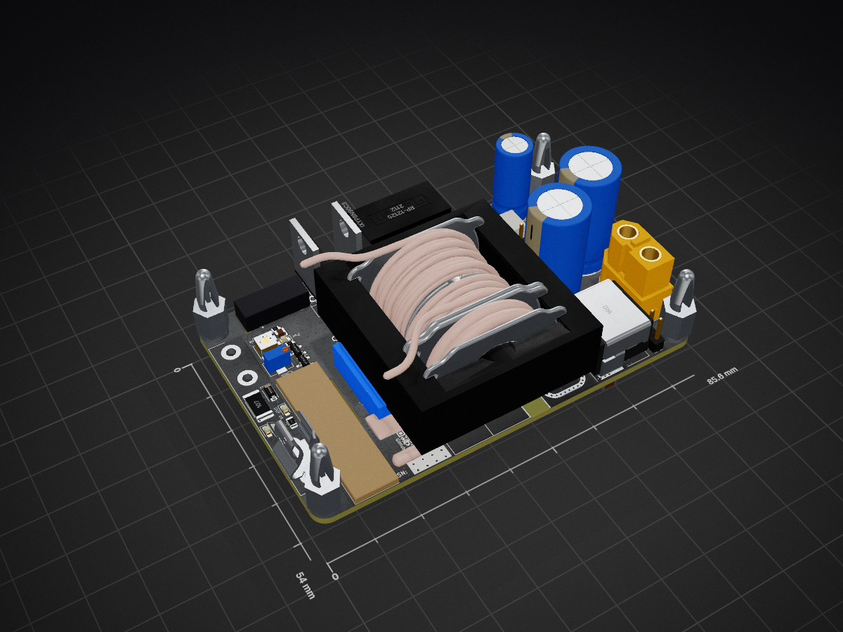
An open source credit card sized DC/DC converter to convert up to 600 V to 24 V in a energy-, cost- and space efficient way.
16 parts161CERN-OHL-W-2.0
 Rootthecause/DCDC161
An open source credit card sized DC/DC converter to convert up to 600 V to 24 V in a energy-, cost- and space efficient way.
DCDCv9-3 is an open-source printed circuit board by Rootthecause, from the Rootthecause/DCDC repository on GitHub, published under the CERN-OHL-W-2.0 licence. It is a 4-layer board of 85.6 × 54 mm with 216 parts on 108 nets, routed with 682 tracks and 744 vias.
It is built around the ACPL-217-50AE, PMV20ENR and CDSOD323-T12, with the BSC027N06LS5ATMA1, IMBG65R050M2HXTMA1 and SS1H10-M3 among its other parts. Its parts include 75 resistors, 57 capacitors, 18 diodes, 9 transistors and 7 connectors. It belongs with the power boards of this library.


Dear Formula Student Teams,
I've designed a High Voltage DC/DC Converter to replace our LV Battery. Feel free to use it as well!
Although this design (and previous versions) have passed two times FSG scrutineering and have been operating without any issues for over 6 months, always manufacture at your own risk!
If you encountered any bugs or have suggestions for improvement, please use the GitHub issues form. For discussions and technical questions, kindly use the discussion bord.
This design is published as open-source hardware under the CERN-OHL-W license and can be found on GitHub: https://github.com/Rootthecause/DCDC
If you had early access to this GitHub page or received any files from me directly, please do not share or publish them, as I don't want others to share files which may be incomplete or contain errors.
Have fun! Do not lick things with spark symbols on :)
Best regards, Rootthecause / Liv
March 10, 2026: Thanks for giving this repro more than 100 stars! ⭐️
| Date YYMMDD | Description |
|---|---|
| 260812 | Urgent notice: The distance between F1 and RV1 is too small, which can lead to a arc on the HV side while the DCDC is enabled. As long as both components do not touch each other conformal coating would prevent the insulation fault, however the actual spacing is influenced by mechanical tolerances. As a hotfix, isolating glue can be used to fill the gap and/or low profile fuse clips (currently untested, should be less wide). The current spacings on the top copper layer between the components are sufficinet with conformal coating. More details on this issue will be added to the Build Notes soon. |
| 260730 | Currently used resonant C0G capacitors might cause converter failures. See v9-3 Build Notes for more details. |
| 260609 | Added new v9-4_dev branch. This version is currently untested and not recommended for use. Some components were improved, like D14, U1, U11, Q8, Q9, Q10, Q11. SR FETs have more vias and 20% larger cooling surface. Increased TS side control voltage from 12V to 15V for lower conduction losses. |
| 260326 | Update on v10 development currently being slowed down due to transformer issues. |
| 260314 | Release of the v9-3r1.4 update. Fixes many smaller issues and probably issue #10. See releases for more details. |
| 260129 | First public v10 schematic, see v10 development, also contains a timeline and small v9-3 update |
| 260104 | New year's update on v10 development |
| 251130 | Update on v10 development, added  for faster communication. |
| 250915 | IMPORTANT NOTICE: There was a complaint about the converter not being rules conform. Due to other personal priorities it might take some weeks to solve the addressed points. There is also the chance of some points unable to be resolved for the Version 9-3r. See issue#10 for further details. |
| 250806 | Announcing the v10 development - ideas welcome! Read more here. DCDCv10 survey. |
| 250718 | A bad F_min setting lead to repeatable FET destruction, please re-read the Build Guide Pages 35/36 if you've set up your replica before this change. See issue#8 |
| File | ||
|---|---|---|
| Documentation [PDF] | ENGLISH | GERMAN [Discontinued*] |
| Build Guide [PDF] | ENGLISH | GERMAN [Discontinued*] |
| Data sheet [PDF] | ENGLISH | - |
| KiCAD Files | ENGLISH | - |
| Schematic [PDF] | ENGLISH | - |
| LTspice Simulation | ENGLISH | - |
| Measurements Table [xlsx] | ENGLISH | - |
| Scrutineering Support Presentation [PPTX] | ENGLISH | - |
*will not be updated after the DCDCv9-3r1.4 release (March 14, 2026).
Always check the latest release before ordering!
There are new releases for every significant hardware change.
I do not recommend ordering from the latest repro clone, as it might contain unfinished hardware changes. However, simulation files or documents might be more recent.
This project is for anyone who is keen to build a DC/DC converter for powering low voltage devices from high voltages or for research.
Unfortunately, it's currently not a simple one-day-build (maybe 1-2 days for building and 1-2 Weeks for testing), but I'm working on it, making it as accessible as possible.
The skillset required ranges from soldering SMD components, SLA-Printing to sanding ferrite cores and winding a transformer (sanding is currently not needed anymore).
The documentation not only contains explanations of many components, but also detailed written assembly instructions.
I might also record a few instruction videos if there is a demand.
Stick with it - the results speak for themselves.
The DCDCv9-3 is a galvanically isolated DC/DC converter, designed to convert voltages from 200 V to 600 V down to 24 V with max. 500 W continuous output power. The low weight of 167 grams and the small footprint of a credit card (85.6 x 54 mm) are well suited to the automotive industry for supplying low-voltage systems from HV Batteries. The dynamic operating frequency between 90 and 200 kHz ensures high efficiency for various loads as well as good EMI compliance due to the resonant LLC soft switching topology. Customized versions allow output voltages from 12 V to 48 V.
Features
The main goal of this project is to create a universal approach for safe and efficient conversion of voltages. At the moment, the converter can accept any input voltage up to at least 600V if UVP/OVP and component Values are chosen correctly. On the output side, the step-down regulator (65V) is the limiting factors. A VIPER06 IC could be used to achieve HV stepdown, or depending on the input voltage, the stepdown could be could be shifted to the input side. This could also allow a self-starting converter to be used as an SMPS in combination with a PFC. Another approach would be a bidirectional design so that the stepdown is on the lower voltage side. Since active rectification is already implemented, bidirectional conversion could be possible given the right IC. With the current development and rise of GaN MOSFETs, a converter with PCB transformer in the MHz range might also be possible.
Last updated: June 24, 2026
Want to add your team to this list (publicly or anonymously)?
Send me a DM on Reddit.
Thanks!
| Qty | Value | Footprint | References |
|---|---|---|---|
| 17 | 10k | DCDC-Footprints:R_0603_1608Metric | R5, R7, R11, R15, R16, R21, R23, R30, R33, R40, R43, R51, R52, R55, R57, R63 +1 |
| 9 | 1nF | DCDC-Footprints:C_0603_1608Metric | C16, C49, C50, C51, C52, C53, C55, C56, C57 |
| 7 | 2.2k | DCDC-Footprints:R_0603_1608Metric | R8, R10, R22, R29, R38, R48, R49 |
| 6 | 100k | DCDC-Footprints:R_0603_1608Metric | R26, R45, R47, R53, R67, R70 |
| 6 | 22uF | DCDC-Footprints:C_0805_2012Metric | C8, C12, C18, C27, C42, C54 |
| 6 | TestPoint | DCDC-Footprints:TestPoint_Pad_D0.8mm_DC-DC | TP1, TP2, TP3, TP4, TP5, TP6 |
| 5 | 10uF | DCDC-Footprints:C_1210_3225Metric | C20, C21, C22, C23, C24 |
| 5 | 1k | DCDC-Footprints:R_0603_1608Metric | R4, R39, R41, R59, R61 |
| 5 | 1uF | DCDC-Footprints:C_0603_1608Metric | C17, C19, C25, C31, C45 |
| 5 | Conn_01x02_Male | DCDC-Footprints:PinHeader_1x02_P2.54mm_Vertical | J2, J4, J6, J7, J8 |
| 5 | Green | DCDC-Footprints:LED_0603_1608Metric_Pad1.05x0.95mm_HandSolder | D3, D4, D5, D6, D7 |
| 5 | PMV20ENR | DCDC-Footprints:SOT-23 | Q1, Q2, Q5, Q6, Q7 |
| 4 | 1N4448 | DCDC-Footprints:D_SOD-123 | D2, D10, D17, D18 |
| 4 | 2.2uF | DCDC-Footprints:C_0805_2012Metric | C2, C15, C40, C41 |
| 4 | 5.6nF | DCDC-Footprints:C_1210_3225Metric | C34, C35, C36, C37 |
| 3 | 10nF | DCDC-Footprints:C_0603_1608Metric | C30, C32, C48 |
| 3 | 10uF | DCDC-Footprints:C_0805_2012Metric | C5, C33, C46 |
| 3 | 22nF | DCDC-Footprints:C_0603_1608Metric | C26, C44, C47 |
| 3 | 33k | DCDC-Footprints:R_0603_1608Metric | R28, R34, R66 |
| 3 | 47 | DCDC-Footprints:R_1206_3216Metric | R6, R14, R20 |
| 3 | 470k | DCDC-Footprints:R_0603_1608Metric | R18, R27, R50 |
| 3 | 470pF | DCDC-Footprints:C_1206_3216Metric | C7, C10, C39 |
| 3 | CDSOD323-T12 | DCDC-Footprints:D_SOD-323 | D8, D15, D16 |
| 3 | HV_Logo_1 | DCDC-Footprints:HV_Logo_small | HV_Logo_1, HV_Logo_1, HV_Logo_1 |
| 3 | LM2904BIDDFR | DCDC-Footprints:SOT-23-8_DC-DC_v9 | U6, U10, U14 |
| 3 | VS-E7FX0212-M3/I | DCDC-Footprints:D_SMF | D11, D12, D14 |
| 2 | 1 nF | DCDC-Footprints:C_1206_3216Metric | C6, C9 |
| 2 | 10 | DCDC-Footprints:R_1206_3216Metric | R56, R58 |
| 2 | 10 | DCDC-Footprints:R_0603_1608Metric | R73, R74 |
| 2 | 100 | DCDC-Footprints:R_1206_3216Metric | R13, R19 |
| 2 | 100M | DCDC-Footprints:R_2512_6332Metric_Pad1.40x3.35mm_HandSolder | R1, R71 |
| 2 | 100M | DCDC-Footprints:R_0603_1608Metric | R62, R69 |
| 2 | 100nF | DCDC-Footprints:C_0603_1608Metric | C14, C28 |
| 2 | 2200uF | DCDC-Footprints:CP_Radial_D12.5mm_P5.00mm_symbol_inside | C11, C13 |
| 2 | 27k | DCDC-Footprints:R_0603_1608Metric | R17, R24 |
| 2 | 330k | DCDC-Footprints:R_0805_2012Metric | R2, R72 |
| 2 | 4.7 | DCDC-Footprints:R_1206_3216Metric | R32, R42 |
| 2 | 4.7k | DCDC-Footprints:R_0603_1608Metric | R31, R36 |
| 2 | BSC027N06LS5ATMA1 | DCDC-Footprints:BSC027N06LS5ATMA1 | Q8, Q9 |
| 2 | IMBG65R050M2HXTMA1 | DCDC-Footprints:TO-263-7_TabPin8 | Q10, Q11 |
| 2 | NCP4305DMTTWG | DCDC-Footprints:WDFN-8_2x2mm_P0.5mm | U5, U8 |
| 2 | NetTie_2 | DCDC-Footprints:dummy_net_line_0.5mm | NT1, NT2 |
| 2 | SS1H10 | DCDC-Footprints:D_SMA | D9, D13 |
| 1 | 1.6A | DCDC-Footprints:Fuseholder0,25Zoll_32mm_littlefuse_102_122 | F1 |
| 1 | 1.6M | DCDC-Footprints:R_0603_1608Metric | R68 |
| 1 | 100k | Resistor_SMD:R_0603_1608Metric | R75 |
| 1 | 10M | DCDC-Footprints:R_1206_3216Metric | R54 |
| 1 | 10k | DCDC-Footprints:Potentiometer_Bourns_3214W_Vertical | RV2 |
| 1 | 10uH | DCDC-Footprints:ASPI-4030S | L3 |
| 1 | 120pF | DCDC-Footprints:C_0603_1608Metric | C38 |
| 1 | 1k PTC | DCDC-Footprints:R_0603_1608Metric | TH2 |
| 1 | 1uH | DCDC-Footprints:7443091100_v9.2 | L2 |
| 1 | 20 | DCDC-Footprints:R_1206_3216Metric | R46 |
| 1 | 20A | DCDC-Footprints:Bel_SMCF_Fuse_2410_6125Metric | F3 |
| 1 | 20k | DCDC-Footprints:Potentiometer_Bourns_PVG3G | RV1 |
| 1 | 22nF | DCDC-Footprints:R76UI22205050J | C3 |
| 1 | 240k | DCDC-Footprints:R_0603_1608Metric | R25 |
| 1 | 2uF | DCDC-Footprints:MKP1848520704K2 | C1 |
| 1 | 3.0k | DCDC-Footprints:R_0603_1608Metric | R3 |
| 1 | 3.3nF | DCDC-Footprints:C_Disc_D12.5mm_W5.0mm_P10.00mm | C4 |
| 1 | 3.8V 25F Supercap | DCDC-Footprints:CP_Radial_D8.0mm_P3.50mm | C_start1 |
| 1 | 330k | DCDC-Footprints:R_0603_1608Metric | R35 |
| 1 | 4.7uH | DCDC-Footprints:ASPI-4030S | L1 |
| 1 | 43650-0315 | Samacsys:43650-03YY_151617 | J1 |
| 1 | 470nF | DCDC-Footprints:C_0603_1608Metric | C43 |
| 1 | 47k | DCDC-Footprints:R_0603_1608Metric | R37 |
| 1 | 47pF | DCDC-Footprints:C_0603_1608Metric | C29 |
| 1 | 500mA | DCDC-Footprints:NANO-0154-OMNI-BLOK-Fuse-Holder | F2 |
| 1 | 510 | DCDC-Footprints:R_0603_1608Metric | R44 |
| 1 | 510k | DCDC-Footprints:R_0603_1608Metric | R65 |
| 1 | 820k | DCDC-Footprints:R_0603_1608Metric | R64 |
| 1 | 82k | DCDC-Footprints:R_0603_1608Metric | R60 |
| 1 | 910 | DCDC-Footprints:R_0603_1608Metric | R12 |
| 1 | ACPL-217-50AE | DCDC-Footprints:SOIC-4_4.55x2.6mm_P1.27mm | U9 |
| 1 | Conn_01x02 | DCDC-Footprints:Molex_Micro-Fit_3.0_43650-0215_1x02_P3.00mm_Vertical_combined2.54pinheader | J3 |
| 1 | DIY Transformer ETD 39 | DCDC-Footprints:Transformer_ETD39_uprightV3.6 (PSS 24V) | T1 |
| 1 | Designed | DCDC-Footprints:Designed by Rootthecause | G*** |
| 1 | Fan Voltage Select | DCDC-Footprints:SolderJumper-3_P1.3mm_Open_RoundedPad1.0x1.5mm_NumberLabels | JP1 |
| 1 | GaN GND2 | DCDC-Footprints:TestPoint_Pad_D0.8mm_DC-DC | TP8 |
| 1 | HV_Orange | DCDC-Footprints:LED_0603_1608Metric_Pad1.05x0.95mm_HandSolder | D1 |
The 197 most common of 216 parts.
It measures 85.6 × 54 mm and has 4 copper layers, 1.6 mm thick.
216 parts, built around the ACPL-217-50AE, PMV20ENR, CDSOD323-T12 and BSC027N06LS5ATMA1. The full list of its parts is on this page, with links to each part's symbol and footprint where PCBKit's library has them.
From the Rootthecause/DCDC repository on GitHub, at the commit this page was made from: the board is kicad/DCDCv9-3.kicad_pcb and its schematic documentation/ESF/DCDCv9-3_ESF KiCAD/DCDCv9-3_ESF.kicad_sch. PCBKit opens the board in the browser, with nothing to install.
Its repository publishes it under the CERN-OHL-W-2.0 licence: you may reuse it on that licence's terms (keep the author's notice, and for a copyleft licence share your changes alike).
Rootthecause/DCDC
An open source credit card sized DC/DC converter to convert up to 600 V to 24 V in a energy-, cost- and space efficient way.

Rootthecause/DCDC
An open source credit card sized DC/DC converter to convert up to 600 V to 24 V in a energy-, cost- and space efficient way.


oro-os/link
The Oro OS CI/CD pipeline including PCBs, CAD files, firmware and server infrastructure

kbx81/kbxLEDController-16ch
kbx's 16-channel ESP-32 Powered LED Strip Controller


