

2 layers49.5 × 42.5 mm

 RobertGawron/SemiconductorRadioactivityDetector29
Nuclear radiation sensor with photodiode as a detector. Photodiode doesn't require high voltages as GM tubes do. Smaller size makes better resolution. Side effect is electronic must be more sensitive.
SemiconductorRadioactivityDetector is an open-source printed circuit board by RobertGawron, from the RobertGawron/SemiconductorRadioactivityDetector repository on GitHub, published under the GPL-3.0 licence. It is a 2-layer board of 90 × 55 mm with 43 parts on 28 nets, routed with 148 tracks and 15 vias.
It is built around the LM358 and BPW34. Its parts include 13 resistors, 12 capacitors, 3 ICs, 3 diodes and 3 connectors. It belongs with the sensors and measurement boards of this library.
The digital output is 12V in the high state and 0V in the low state, which is not very useful for the 3.3V logic microcontroller I'm using for data acquisition. To solve this, I built a simple converter on an additional PCB.

Here, you can see it soldered.
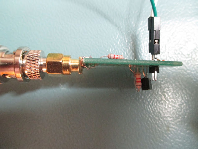
What I like about these SMA female sockets is that they can be soldered to the edge of the PCB (as shown below), making them mechanically stable without the need to drill holes, unlike the regular mounting method.
Note that there is no PCB design; a breadboard is used for assembly.
| Qty | Value | Footprint | References |
|---|---|---|---|
| 7 | 10k | Resistors_SMD:R_0805_HandSoldering | R1, R2, R5, R7, R9, R10, R11 |
| 5 | 100n | Capacitor_SMD:C_0805_2012Metric | C1, C3, C4, C5, C8 |
| 4 | 12V | SemiconductorRadioactivityDetector:A23Single | BT1, BT2, BT3, BT4 |
| 3 | BPW34 | Diodes_THT:D_DO-35_SOD27_P5.08mm_Vertical_KathodeUp | D1, D2, D3 |
| 3 | MountingHole_Pad | Mounting_Holes:MountingHole_3.5mm_Pad | H1, H2, H3 |
| 2 | 100n | Capacitors_SMD:C_0805_HandSoldering | C2, C9 |
| 2 | Conn_Coaxial | Connector_Coaxial:BNC_PanelMountable_Vertical | J1, J2 |
| 2 | OPA333xxD | Housings_SOIC:SOIC-8_3.9x4.9mm_Pitch1.27mm | U1, U2 |
| 2 | not mounted | Resistors_SMD:R_0805_HandSoldering | R12, R13 |
| 1 | 0R | Resistors_SMD:R_0805_HandSoldering | R3 |
| 1 | 10G | Resistors_SMD:R_0805_HandSoldering | R4 |
| 1 | 10M | Resistors_SMD:R_0805_HandSoldering | R8 |
| 1 | 10k | Resistors_THT:R_Axial_DIN0207_L6.3mm_D2.5mm_P10.16mm_Horizontal | R6 |
| 1 | 1n | Capacitor_SMD:C_0805_2012Metric | C7 |
| 1 | 1u/16v | Capacitor_Tantalum_SMD:CP_EIA-3216-18_Kemet-A | C12 |
| 1 | 2p2 | Capacitor_SMD:C_0805_2012Metric | C6 |
| 1 | 4p7+2p2 | Capacitors_SMD:C_0805_HandSoldering | C10 |
| 1 | Conn_01x02_Pin | Connector_PinHeader_2.54mm:PinHeader_1x02_P2.54mm_Vertical | J3 |
| 1 | LM358 | Package_SO:SOIC-8_3.9x4.9mm_P1.27mm | U3 |
| 1 | R_Potentiometer_Trim | Potentiometer_THT:Potentiometer_Bourns_3296W_Vertical | RV1 |
| 1 | solder bridge | Capacitor_SMD:C_0805_2012Metric | C11 |
| 1 | u68 | Inductor_SMD:L_1812_4532Metric | L1 |
It measures 90 × 55 mm and has 2 copper layers, 1.6 mm thick.
43 parts, built around the LM358 and BPW34. The full list of its parts is on this page, with links to each part's symbol and footprint where PCBKit's library has them.
From the RobertGawron/SemiconductorRadioactivityDetector repository on GitHub, at the commit this page was made from: the board is Hardware/SemiconductorRadioactivityDetector/SemiconductorRadioactivityDetector.kicad_pcb and its schematic Hardware/LogicLevelConverter/LogicLevelConverter.kicad_sch. PCBKit opens the board in the browser, with nothing to install.
Its repository publishes it under the GPL-3.0 licence: you may reuse it on that licence's terms (keep the author's notice, and for a copyleft licence share your changes alike).

abhictrl/IEEE-HOPE-FSO
A laser-based audio communication link for the Howard University IEEE H.O.P.E. Project.


QuantumVillage/UncutGem
A prototype Full Stack fully Open Source NV Center Diamond Magnetometer

Roboy/HTC_Vive_Sensors
Schematics and PCB designs for our custom Vive sensors based on a quad op-amp chip rather than discrete transistors.

meetjestad/mjs_pcb
This repository contains various versions of the sensor station PCB used by Meetjestad.
