
2 layers11.7 × 11.2 mm
PressureSensor
rivertechlabs/suspendedsedimentsensor
:ocean: 3D-printed, open-source suspended sediment sensor for river network monitoring (prototype 3.0)
7 parts12AGPL-3.0
:ocean: 3D-printed, open-source suspended sediment sensor for river network monitoring (prototype 3.0)
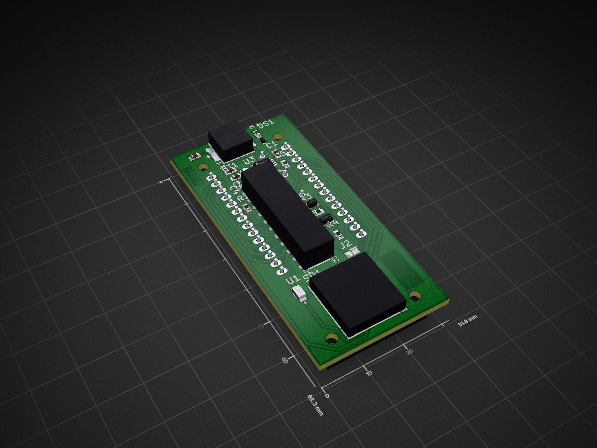
MainPCB is an open-source printed circuit board by rivertechlabs, from the rivertechlabs/suspendedsedimentsensor repository on GitHub, published under the AGPL-3.0 licence. It is a 2-layer board of 31.7 × 68.3 mm with 23 parts on 24 nets, routed with 323 tracks and 0 vias.
It is built around the PCF85263ATT/AJ, 2N7002LT1G and HSMH-C190. Its parts include 7 resistors, 4 capacitors, 3 ICs, 2 connectors and 1 transistor. It belongs with the sensors and measurement boards of this library.


This sensor is prototype 3.0 (or "version Ötz-T"). The previous prototype 2.0 (or "first version") is found in this repo (new repo because I consider the two versions different enough).
This sensor was published in HardwareX! Read Ötz-T: 3D-printed open-source turbidity sensor with Arduino shield for suspended sediment monitoring.
Improvements on this version:
A 3D-printed, open-source suspended sediment sensor for river network monitoring.
This repo is dedicated to the open-source turbidity sensor. More info can be found here:
This repo contains several items to build the current prototype of the open-source turbidity sensor including:
There are two codes in the Code folder: main.ino and set_time.ino. Please follow the instructions in set time.ino about changing the date in the program. After the program has flashed, every time the Arduino restarts (disconnect and reconnect to power) it will restart the RTC time to the original compile time of the set time.ino program. To mitigate this issue, the next program, main.ino, can be immediately flashed without disconnecting power or set time.ino can be re-flashed after commenting-out line 79 (“setPCF85263();”). Follow by flashing main.ino onto the Arduino. Please note that additional libraries may need to be downloaded and added to your library (e.g. the MS5803-05 external library). The main.ino program was written to take a measurement every hour (one measurement is an average of 15 measurements) to conserve battery, but this can be changed in the code if you require higher temporal resolution to capture larger variability e.g. from flushing of sediment from a dam.
Here you will find the printer files (.gcode) and the PrusaSlicer files (.3mf). The CAD files were exported as .stp and imported into the PrusaSlicer program (free). See the .3mf files to understand the settings we used in PrusaSlicer for optimal printing. The main settings were:
The .3mf files were exported as .gcode files and then printed on a Prusa I3 Mk3 and/or Mk3S Filament Printer.
We have provided the Gerber files to directly order the PCBs. Alternatively, the .PcbDoc and .SchDoc files can be opened in Altium (the eductional license can be obtained for free) where you can export your own Gerber files. Finally, the schematic and PCB files were also provided as KiCad files so that they can be viewed and edited without Altium.
In this folder we have the original CAD files (as STEP) so that they can be downloaded and adjusted for your project.
For questions, please email me at droujko@ifu.baug.ethz.ch or @rivertechjess on Twitter :bird:
| Qty | Value | Footprint | References |
|---|---|---|---|
| 4 | 10k | Vault:RESC2013X60X35NL10T20 | R1, R2, R4, R5 |
| 2 | 100nF | Vault:CAPC2013X140X50NL20T25 | C1, C2 |
| 2 | 10pF | Vault:CAPC2013X115X51NL20T26 | C3, C4 |
| 2 | Comment | C:_Users_Public_Documents_Altium_AD21_Library_Miscellaneous Devices.IntLib_AXIAL-0.3 | Designator1, Designator2 |
| 1 | 2N7002LT1G | Vault:ONSC-SOT-23-3-318-08_V | Q1 |
| 1 | 32.768KHZ | Vault:FP-ABS05-MFG | Y1 |
| 1 | 330R | Vault:RESC2013X60X40NL20T25 | R3 |
| 1 | 330R | Vault:RESC2013X60X35LL10T20 | R7 |
| 1 | 473521001 | Vault:MOLX-473521001_V | SD1 |
| 1 | 61002221121 | Vault:61002221121 | J1 |
| 1 | AL5809-50P1-7 | Vault:DIOD-POWERDI123-2_B_V | U1 |
| 1 | Arduino MKR 1310 | SwS.PcbLib:ArduinoMKR | U2 |
| 1 | HSMH-C190 | Vault:AVAG-HSMX-C190_V | DS1 |
| 1 | Jumper_2W | SwS.PcbLib:2w_Jumper | J2 |
| 1 | LR621 | Vault:FP-2998-MFG | BT1 |
| 1 | PCF85263ATT/AJ | Vault:FP-SOT505-1-IPC_B | U3 |
| 1 | n.c. | Vault:RESC2013X60X35NL10T20 | R6 |
It measures 31.7 × 68.3 mm and has 2 copper layers, 1.6 mm thick.
23 parts, built around the PCF85263ATT/AJ, 2N7002LT1G and HSMH-C190. The full list of its parts is on this page, with links to each part's symbol and footprint where PCBKit's library has them.
From the rivertechlabs/suspendedsedimentsensor repository on GitHub, at the commit this page was made from: the board is PCB/MainPCB/MainPCB.kicad_pcb and its schematic PCB/IRDiode/IR_Diode_PCB.kicad_sch. PCBKit opens the board in the browser, with nothing to install.
Its repository publishes it under the AGPL-3.0 licence: you may reuse it on that licence's terms (keep the author's notice, and for a copyleft licence share your changes alike).
rivertechlabs/suspendedsedimentsensor
:ocean: 3D-printed, open-source suspended sediment sensor for river network monitoring (prototype 3.0)

rivertechlabs/suspendedsedimentsensor
:ocean: 3D-printed, open-source suspended sediment sensor for river network monitoring (prototype 3.0)

rivertechlabs/suspendedsedimentsensor
:ocean: 3D-printed, open-source suspended sediment sensor for river network monitoring (prototype 3.0)

niksrajendra/stm8-bootloader-extended
STM8 bootloader designed to work with any available communication interface and configure for different feature like secure, unsecure bootloader.


eihli/morse-mesh
This is the current hardware source for future Morse Mesh revisions. It is a professionally reviewed redraw of the frozen, fabricated v1 board, not a pin-compatible replacement: notably, KEYIN moved from v1 PA0 to v2…

