2 layers50 × 23.2 mm
Analog
hoglet67/RGBtoHDMI
Bare-metal Raspberry Pi project that provides pixel-perfect sampling of Retro Computer RGB/YUV video and conversion to HDMI
32 parts1kGPL-3.0
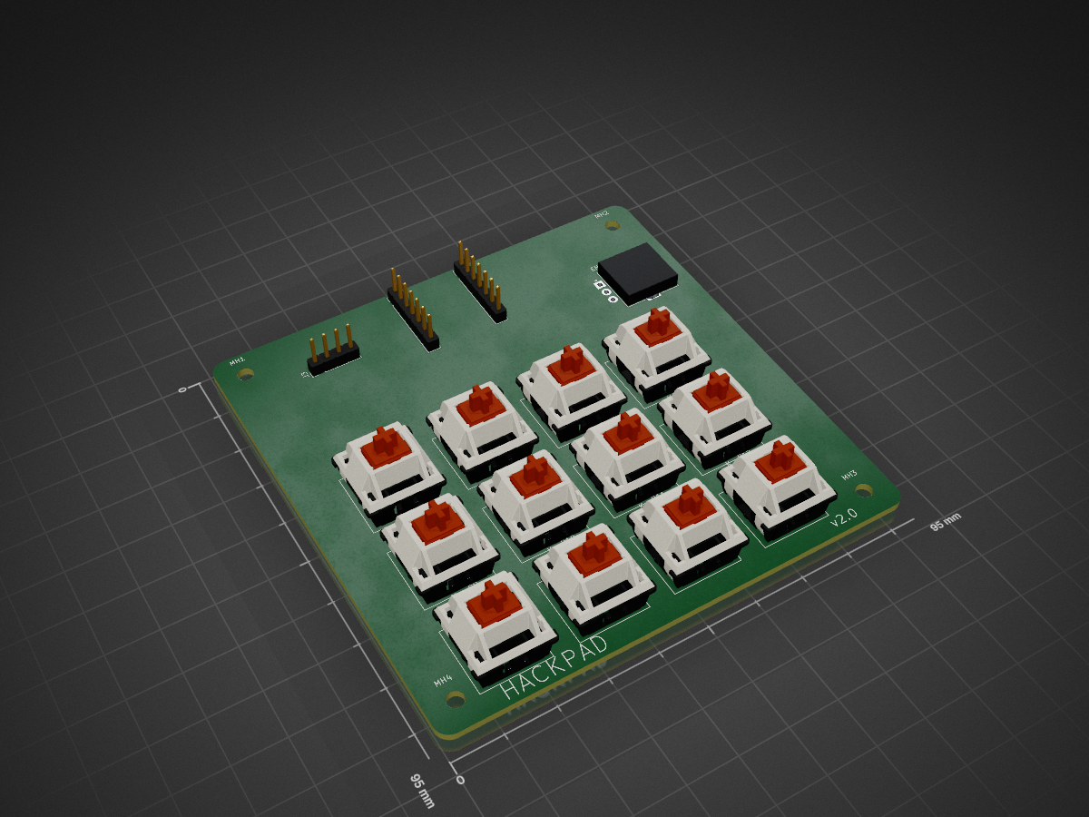
 rishith-c/hackpad
4-key macropad + EC11 encoder + OLED, XIAO RP2040, KMK firmware. Submitted to Hack Club Hackpad YSWS.
Hackpad is an open-source printed circuit board by rishith-c, from the rishith-c/hackpad repository on GitHub, published under the MIT licence. It is a 2-layer board of 95 × 95 mm with 32 parts on 26 nets, routed with 43 tracks and 0 vias.
Its parts include 12 diodes, 12 switches and 3 connectors. It belongs with the keyboards and input and lEDs and displays boards of this library.
A 12-key macropad with a rotary encoder and an OLED display, built on a Seeed XIAO RP2040 and running KMK firmware. Submitted to Hack Club's Hackpad You Ship, We Ship program.
v2 — the most loaded build that fits the Hackpad rules at once: 12 MX keys, 1 EC11 rotary encoder, 1 OLED display, and every usable GPIO on the XIAO consumed (11 / 11). 13 inputs, well under the 16-input cap; 95 × 95 mm board, well inside the 100 × 100 mm size cap.
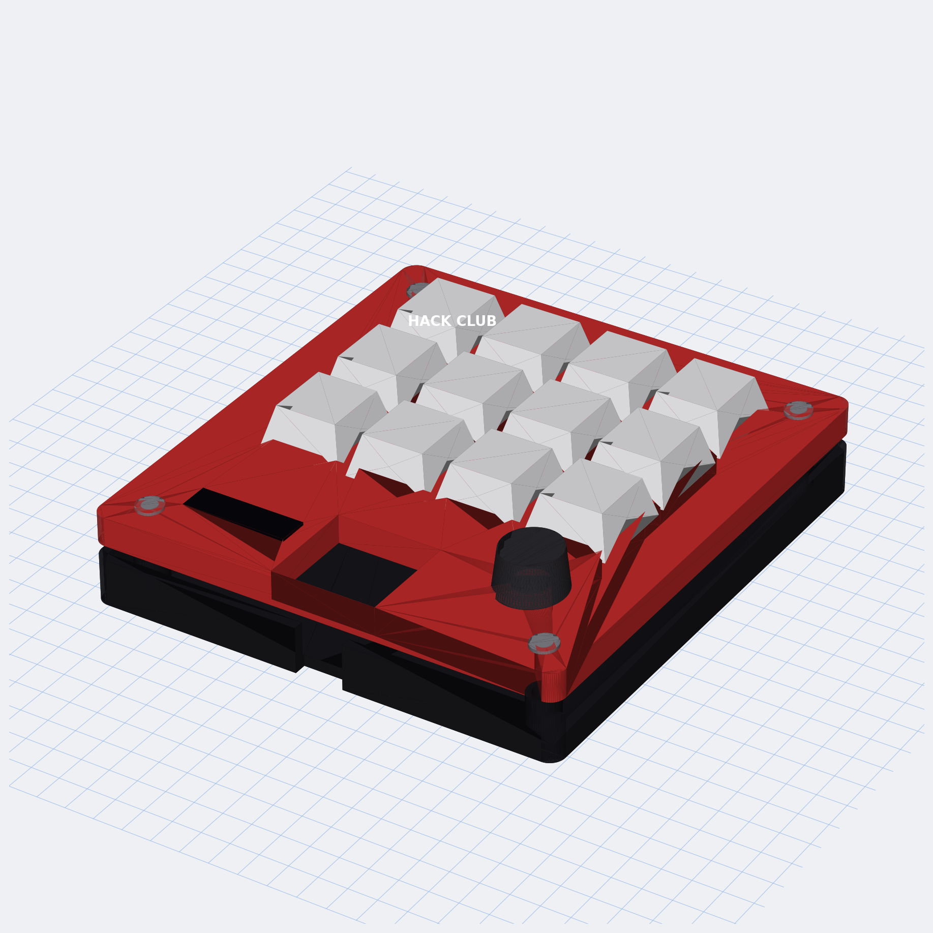
Full assembled view in cad/assembled-model.step —
GitHub renders the STEP inline. STL version in
cad/assembled-model.stl.
Printable + hardware parts (all generated by
build_scripts/build_case.py):
| Part | STL | STEP | Notes |
|---|---|---|---|
| Top plate (red, 5 mm) | Top.stl | Top.step | 12 MX cutouts + encoder hole + OLED window + XIAO inspection |
| Bottom tray (black, 8 mm) | Bottom.stl | Bottom.step | 4× heatset bosses + USB-C side cutout |
| M3 × 16 mm SHCS screw (×4) | M3x16_Screw.stl | M3x16_Screw.step | hardware visualization — kit supplies real ones |
| M3 × 5 × 4 mm brass heatset insert (×4) | HeatsetInsert_M3x5x4.stl | HeatsetInsert_M3x5x4.step | hardware visualization — kit supplies real ones |
Case fits within 99 × 99 × 15 mm — well inside Hackpad's 200 × 200 × 100 mm limit. Screwed together with 4 × M3 × 16 mm SHCS bolts into M3 × 5 × 4 mm brass heatset inserts.
Built in KiCad 9 from
pcb/hackpad.kicad_pro. The whole board is
generated programmatically by
build_scripts/build_pcb.py from the netlist
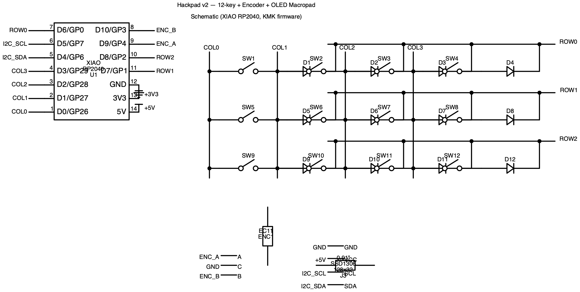
.kicad_pcb byte-for-byte.Schematic:
PCB layout (top and bottom copper):
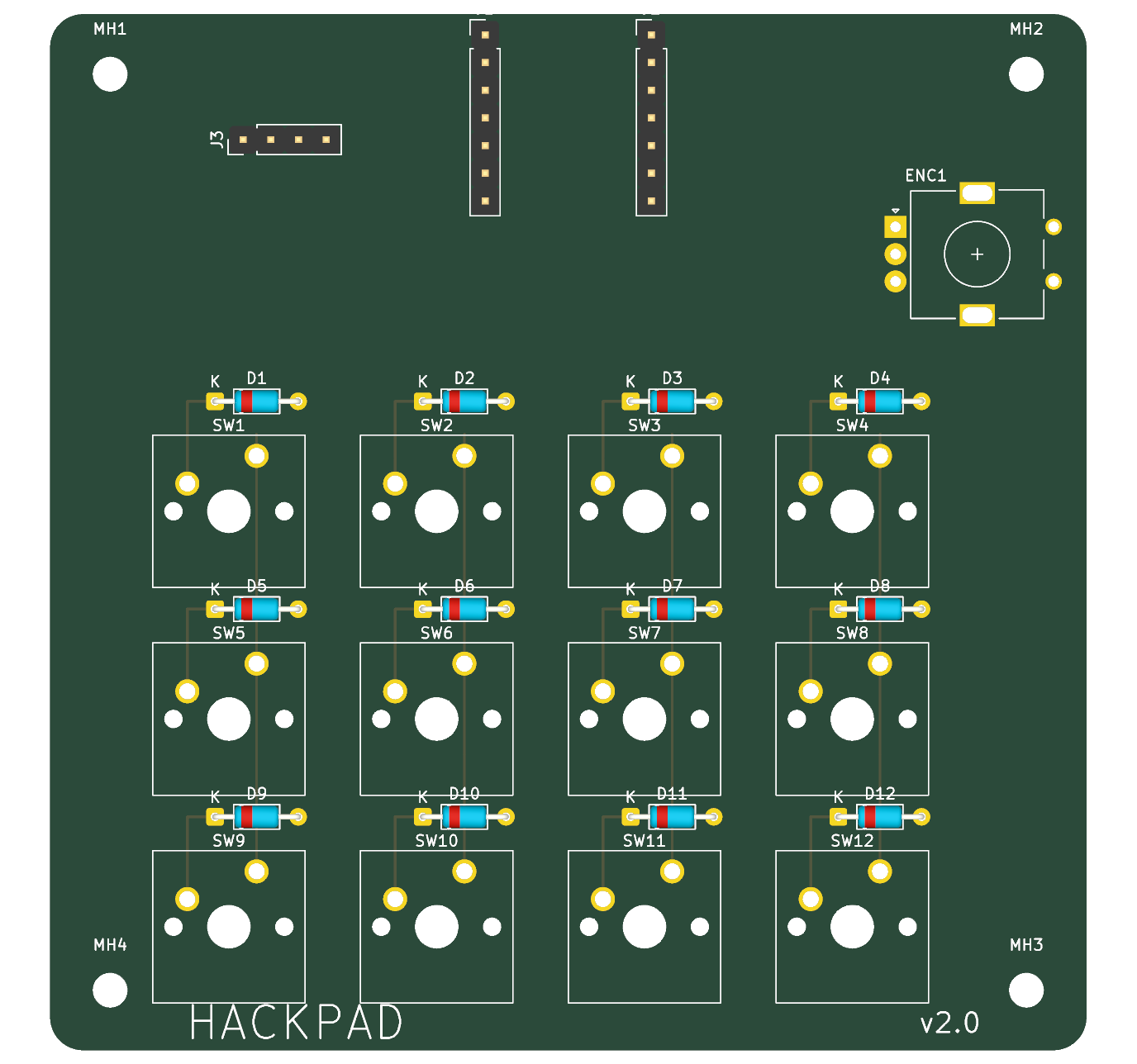
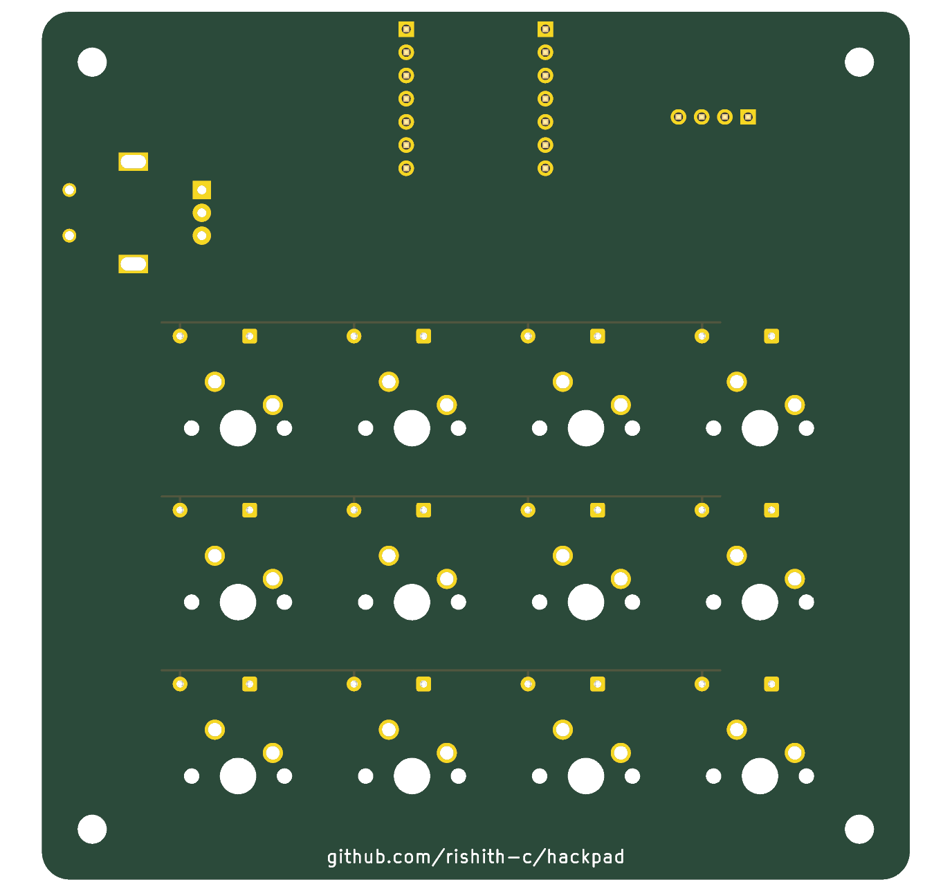
PinHeader_1x07_P2.54mm_Vertical,
OLED on PinHeader_1x04_P2.54mm_Vertical, MountingHole_3.2mm_M3pcb/HOW_TO_FINISH.md for the exact
start/end coordinates of each pull.HACKPAD v2.0 on the front, github.com/rishith-c/hackpad
on the back.kicad-cli pcb drc --severity-error → 0 violations)Gerbers exported and ready for JLCPCB:
production/gerbers.zip.
Order at 2 layers · 1.6 mm · HASL · green.
KMK (CircuitPython). See firmware/README.md for
flashing instructions. Sources in firmware/KMK/:
| File | Purpose |
|---|---|
firmware/KMK/main.py | 4×3 matrix + encoder + OLED setup, 3 keymap layers |
firmware/KMK/code.py | CircuitPython entry point (imports main) |
firmware/KMK/boot.py | disables CIRCUITPY auto-reload while plugged in |
The XIAO RP2040 exposes 11 usable GPIO. All 11 are used.
| XIAO | GPIO | Role |
|---|---|---|
| D0 | GP26 | matrix COL0 (left column) |
| D1 | GP27 | matrix COL1 |
| D2 | GP28 | matrix COL2 |
| D3 | GP29 | matrix COL3 (right column) |
| D4 | GP6 | OLED SDA (I²C1) |
| D5 | GP7 | OLED SCL (I²C1) |
| D6 | GP0 | matrix ROW0 (top row) |
| D7 | GP1 | matrix ROW1 (middle row) |
| D8 | GP2 | matrix ROW2 (bottom row) |
| D9 | GP4 | encoder phase A |
| D10 | GP3 | encoder phase B |
No spare GPIOs. See pcb/DESIGN_NOTES.md for
alternate firmware tweaks (drop OLED for encoder push + RGB; shrink
matrix to 3×3 for a second encoder; etc.) — each one reuses this same
PCB without changes.
See production/BOM.csv. Everything except the
PLA filament is in the Hackpad kit.
production/Top.stl)production/Bottom.stl)├── README.md
├── LICENSE
├── cad/
│ ├── assembled-model.step # full assembly (Hackpad spec)
│ └── assembled-model.stl # same, STL (GitHub interactive viewer)
├── pcb/
│ ├── hackpad.kicad_pro # KiCad project
│ ├── hackpad.kicad_sch # schematic stub (canonical viz in assets/schematic.png)
│ ├── hackpad.kicad_pcb # placed + matrix-routed board
│ ├── netlist.csv # canonical net list
│ ├── placement.csv # per-part X/Y/rotation
│ ├── DESIGN_NOTES.md # build variants / pin budget reasoning
│ └── HOW_TO_FINISH.md # 5-min interactive routing checklist
├── firmware/
│ ├── README.md
│ └── KMK/
│ ├── main.py # KMK firmware (matrix + encoder + OLED, 3 layers)
│ ├── code.py # CircuitPython entry point
│ └── boot.py # boot-time config
├── production/
│ ├── gerbers.zip # for JLCPCB (2 layers, 1.6 mm)
│ ├── Top.step / Top.stl # top plate
│ ├── Bottom.step / Bottom.stl # bottom tray
│ ├── M3x16_Screw.step / .stl # individual screw model (used x4)This repo matches the Hackpad submission requirements:
cad/, pcb/, firmware/, production/, README.md ✅
(matches the Orpheuspad reference)Submission steps:
#hackpad-ships on the Hack Club Slack (link to
this repo + photos from assets/).@alexren. On approval you receive the kit + a $15
grant for JLCPCB PCB fab + a free 3D-printed case from another
Hack Clubber, plus optionally $18 for a soldering iron.# PCB (uses KiCad 9 bundled Python — pcbnew API)
/Applications/KiCad.app/Contents/Frameworks/Python.framework/Versions/Current/bin/python3 build_scripts/build_pcb.py
# Case + screws + assembled model (pip install cadquery)
python3 build_scripts/build_case.py
# Schematic (pip install schemdraw cairosvg; cairo from Homebrew)
DYLD_FALLBACK_LIBRARY_PATH=/opt/homebrew/lib python3 build_scripts/build_schematic.py
# Mockup PNG (pip install cadquery trimesh matplotlib)
python3 build_scripts/build_mockup.py
# Gerbers + drill files, bundled to production/gerbers.zip
mkdir -p /tmp/gerbers && \
/Applications/KiCad.app/Contents/MacOS/kicad-cli pcb export gerbers \
--output /tmp/gerbers/ \
--layers "F.Cu,B.Cu,F.Silkscreen,B.Silkscreen,F.Mask,B.Mask,Edge.Cuts" \
pcb/hackpad.kicad_pcb && \
/Applications/KiCad.app/Contents/MacOS/kicad-cli pcb export drill \
--output /tmp/gerbers/ --excellon-separate-th pcb/hackpad.kicad_pcb && \
( cd /tmp/gerbers && zip /path/to/production/gerbers.zip *.gtl *.gbl *.gto *.gbo *.gts *.gbs *.gm1 *.drl )MIT.
| Qty | Value | Footprint | References |
|---|---|---|---|
| 12 | 1N4148 | D_DO-35_SOD27_P7.62mm_Horizontal | D1, D2, D3, D4, D5, D6, D7, D8, D9, D10, D11, D12 |
| 12 | MX | SW_Cherry_MX_1.00u_PCB | SW1, SW2, SW3, SW4, SW5, SW6, SW7, SW8, SW9, SW10, SW11, SW12 |
| 4 | M3 | MountingHole_3.2mm_M3 | MH1, MH2, MH3, MH4 |
| 1 | EC11 | RotaryEncoder_Alps_EC11E_Vertical_H20mm | ENC1 |
| 1 | OLED | PinHeader_1x04_P2.54mm_Vertical | J3 |
| 1 | XIAO_L | PinHeader_1x07_P2.54mm_Vertical | J1 |
| 1 | XIAO_R | PinHeader_1x07_P2.54mm_Vertical | J2 |
It measures 95 × 95 mm and has 2 copper layers, 1.6 mm thick.
32 parts. The full list of its parts is on this page, with links to each part's symbol and footprint where PCBKit's library has them.
From the rishith-c/hackpad repository on GitHub, at the commit this page was made from: the board is pcb/hackpad.kicad_pcb and its schematic pcb/hackpad.kicad_sch. PCBKit opens the board in the browser, with nothing to install.
Its repository publishes it under the MIT licence: you may reuse it on that licence's terms (keep the author's notice, and for a copyleft licence share your changes alike).
hoglet67/RGBtoHDMI
Bare-metal Raspberry Pi project that provides pixel-perfect sampling of Retro Computer RGB/YUV video and conversion to HDMI

hackclub/OnBoard
💡 Join 1,000 teenagers and make your first PCB with a $100 grant!


octosavvi/ESPKey
Wiegand data logger, replay device and micro door-controller

zmaker/arduino_cookbook
gli sketch del nuovo progetto Arduino Cookbook e dei video di YouTube

murexrobotics/electrical
Highly integrated electronics design and printed circuit boards (PCBs) for the MATE ROV Competition. Attempt the impossible.

swharden/AVR-projects
A collection of standalone AVR projects written in C

hardenedlinux/cheap-pcb
Cheap PCB: Better understanding the current status of hardware supply chain