4 layers
TubesPCB Wijdan
wijdanmkh-insk/Tasks
This is my backups from my exercises and for fun coding. I don't like my files that messing around my main drive so instead save them in my computer, I save them here. It's just for fun.
26 parts
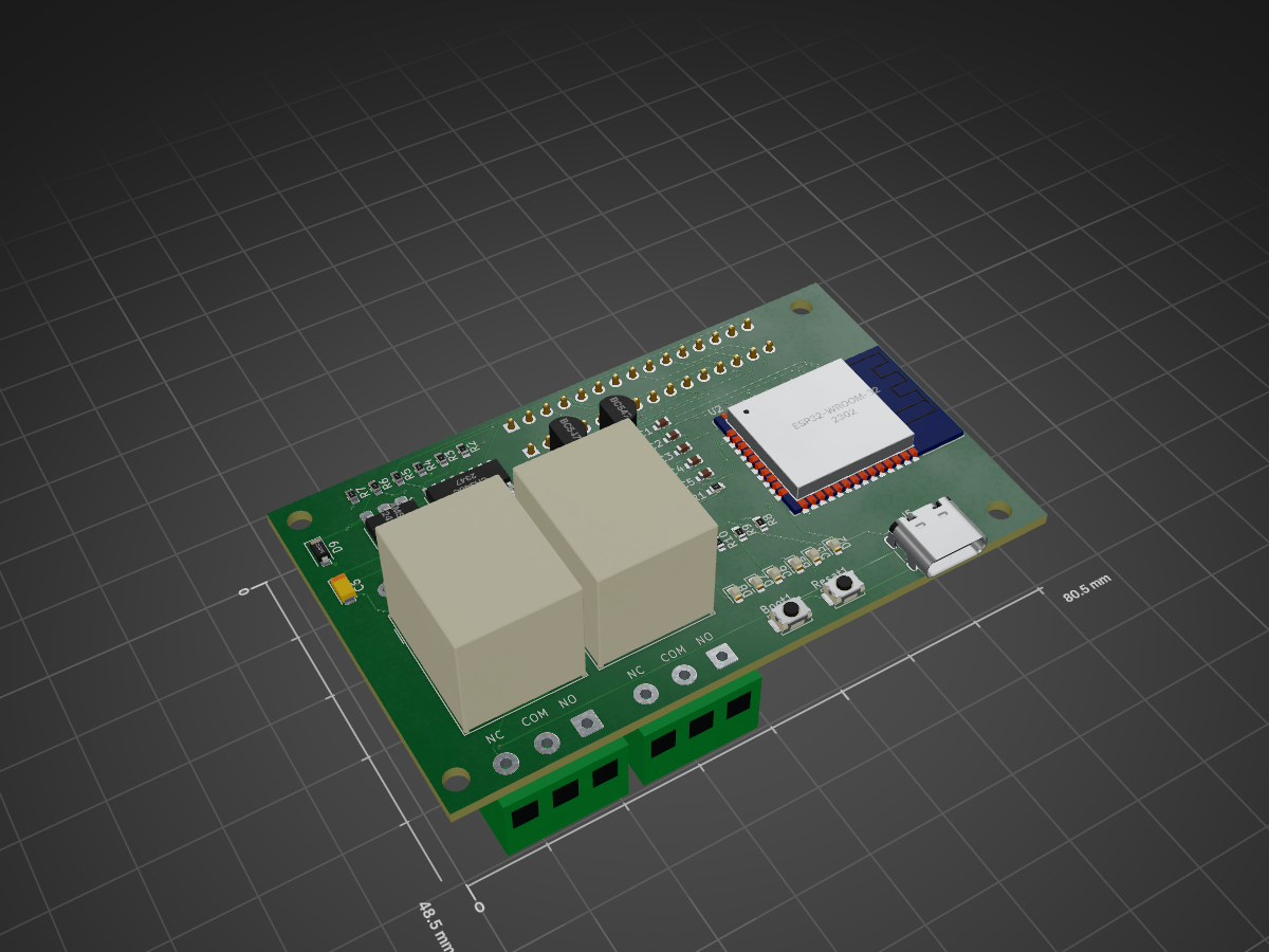
 rayan-e/FT-Solution-PCB
FT Solution PCB2 is an open-source printed circuit board by rayan-e, from the rayan-e/FT-Solution-PCB repository on GitHub. It is a 2-layer board of 80.5 × 48.5 mm with 42 parts on 70 nets, routed with 765 tracks and 84 vias.
It is built around the CH340C, ESP32-WROOM-32 and AMS1117, with the BC547, SS8050 and B5819W among its other parts. Its parts include 11 resistors, 9 diodes, 6 capacitors, 5 connectors and 4 transistors. It belongs with the ESP32 boards of this library.


| Qty | Value | Footprint | References |
|---|---|---|---|
| 5 | 100nf | Capacitor_SMD:C_0603_1608Metric | C1, C2, C3, C4, C5 |
| 4 | 1K | Resistor_SMD:R_0603_1608Metric | R3, R4, R6, R7 |
| 3 | 10K | Resistor_SMD:R_0603_1608Metric | R1, R2, R5 |
| 3 | BLUE | LED_SMD:LED_0603_1608Metric | D2, D5, D7 |
| 3 | RED | LED_SMD:LED_0603_1608Metric | D3, D6, D8 |
| 2 | 1N4007 | Diode_THT:D_DO-41_SOD81_P10.16mm_Horizontal | D1, D4 |
| 2 | 5k1 | Resistor_SMD:R_0603_1608Metric | R9, R10 |
| 2 | BC547 | Package_TO_SOT_THT:TO-92_Inline | Q3, Q4 |
| 2 | Conn_01x15_Pin | Connector_PinHeader_2.54mm:PinHeader_1x15_P2.54mm_Vertical | J2, J4 |
| 2 | FINDER-36.11 | Relay_THT:Relay_SPDT_Finder_36.11 | K1, K2 |
| 2 | SS8050 | Package_TO_SOT_SMD:SOT-23 | Q1, Q2 |
| 2 | SW_Push | Button_Switch_SMD:SW_Push_SPST_NO_Alps_SKRK | Boot1, Resat1 |
| 2 | Screw_Terminal_01x03 | TerminalBlock:TerminalBlock_MaiXu_MX126-5.0-03P_1x03_P5.00mm | J1, J3 |
| 1 | 10uf/16V | Capacitor_Tantalum_SMD:CP_EIA-3216-10_Kemet-I | C6 |
| 1 | 1k | Resistor_SMD:R_0603_1608Metric | R11 |
| 1 | 220R | Resistor_SMD:R_0603_1608Metric | R8 |
| 1 | AMS1117 | Package_TO_SOT_SMD:SOT-223-3_TabPin2 | U3 |
| 1 | B5819W | Diode_SMD:D_SOD-123 | D9 |
| 1 | CH340C | Package_SO:SOIC-16_3.9x9.9mm_P1.27mm | U1 |
| 1 | ESP32-WROOM-32 | RF_Module:ESP32-WROOM-32 | U2 |
| 1 | USB_C_Receptacle_USB2.0_16P | Connector_USB:USB_C_Receptacle_HRO_TYPE-C-31-M-12 | J5 |
wijdanmkh-insk/Tasks
This is my backups from my exercises and for fun coding. I don't like my files that messing around my main drive so instead save them in my computer, I save them here. It's just for fun.

zaidh-mech/PROJECTS
Engineering, robotics, embedded systems, CAD, and PCB projects

moksh-pcb-design/ESP32-WROOM-Development-Board
Custom ESP32-WROOM-32 Development Board designed in KiCad 10 featuring USB Type-C, CH340C USB-UART interface, AMS1117 power regulation and auto-programming circuitry.

7205jmj/Custom-ESP32-WROOM-32-Development-Board
Most ESP32 development boards available in the market include additional features that may not be required for every project.


Adichidrawar/electronics-assessment-IF
Hardware design solution for the Intelligence Factory Hardware/Mechatronics Engineer take-home assessment. Includes a two-board ESP32-based embedded system with a remote IMU sensor board, complete PCB design in KiCad…

arm-n/ESP-WROOM-32-Development-Board
A hardware prototyping project based on the ESP-WROOM-32 module, designed using KiCad. This repository contains the circuit schematic, PCB layout, Gerber manufacturing files, design screenshots, datasheets and…

It measures 80.5 × 48.5 mm and has 2 copper layers, 1.6 mm thick.
42 parts, built around the CH340C, ESP32-WROOM-32, AMS1117 and BC547. The full list of its parts is on this page, with links to each part's symbol and footprint where PCBKit's library has them.
From the rayan-e/FT-Solution-PCB repository on GitHub, at the commit this page was made from: the board is FT_Solution_PCB2.kicad_pcb and its schematic FT_Solution_PCB2.kicad_sch. PCBKit opens the board in the browser, with nothing to install.
Its repository states no licence, so its author keeps all rights: ask rayan-e before reusing the design.