4 layers30 × 23.5 mm
NIMRS-21Pin Decoder
CDFER/NIMRS-21Pin-Decoder
An open source 21-Pin DCC Decoder for model trains
89 parts21

 RaidenTechnology/raiden-s01
Open-hardware ESP32-S3 development board — 4-layer, USB-C, U.FL antenna. KiCad 9, CERN-OHL-P.
Raiden s01 is an open-source printed circuit board by RaidenTechnology, from the RaidenTechnology/raiden-s01 repository on GitHub, published under the CERN-OHL-P-2.0 licence. It is a 4-layer board of 36 × 60 mm with 46 parts on 57 nets, routed with 718 tracks and 121 vias.
It is built around the ESP32-S3FN8 and PRTR5V0U2X. Its parts include 18 capacitors, 7 resistors, 6 connectors, 2 ICs and 2 diodes. It belongs with the radio and wireless boards and the ESP32 boards of this library.


Open-hardware ESP32-S3 development board — designed from scratch in KiCad 9.
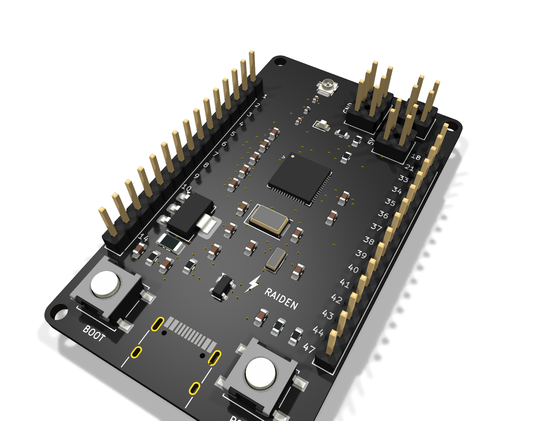
The Raiden S0-1 is a compact 4-layer devkit built around the ESP32-S3FN8 (dual-core Xtensa LX7 @ 240 MHz, Wi-Fi + BLE 5, 8 MB embedded flash). Designed, routed and verified entirely by Raiden Technology.
| MCU | ESP32-S3FN8 (QFN-56, 8 MB flash) |
| USB | USB-C (USB 2.0), ESD-protected (PRTR5V0U2X), 5.1 kΩ CC pull-downs |
| Power | AZ1117C-3.3 LDO, 750 mA PTC resettable fuse, power LED |
| RF | U.FL (IPEX) antenna connector, feed line drawn for 50 Ω single-ended with a pi matching network — see the note below, impedance is not verified |
| Clocks | 40 MHz main crystal (CL = 8 pF) · 32.768 kHz RTC crystal (CL = 12.5 pF) |
| I/O | 2 × 15-pin 2.54 mm headers, BOOT + RESET buttons |
| Board | 4-layer FR-4, 1.6 mm — Sig / GND / +3V3 / Sig stackup, black soldermask |
| Mounting | 4 × M2 holes (NPTH) |
| Top | Bottom |
|---|---|
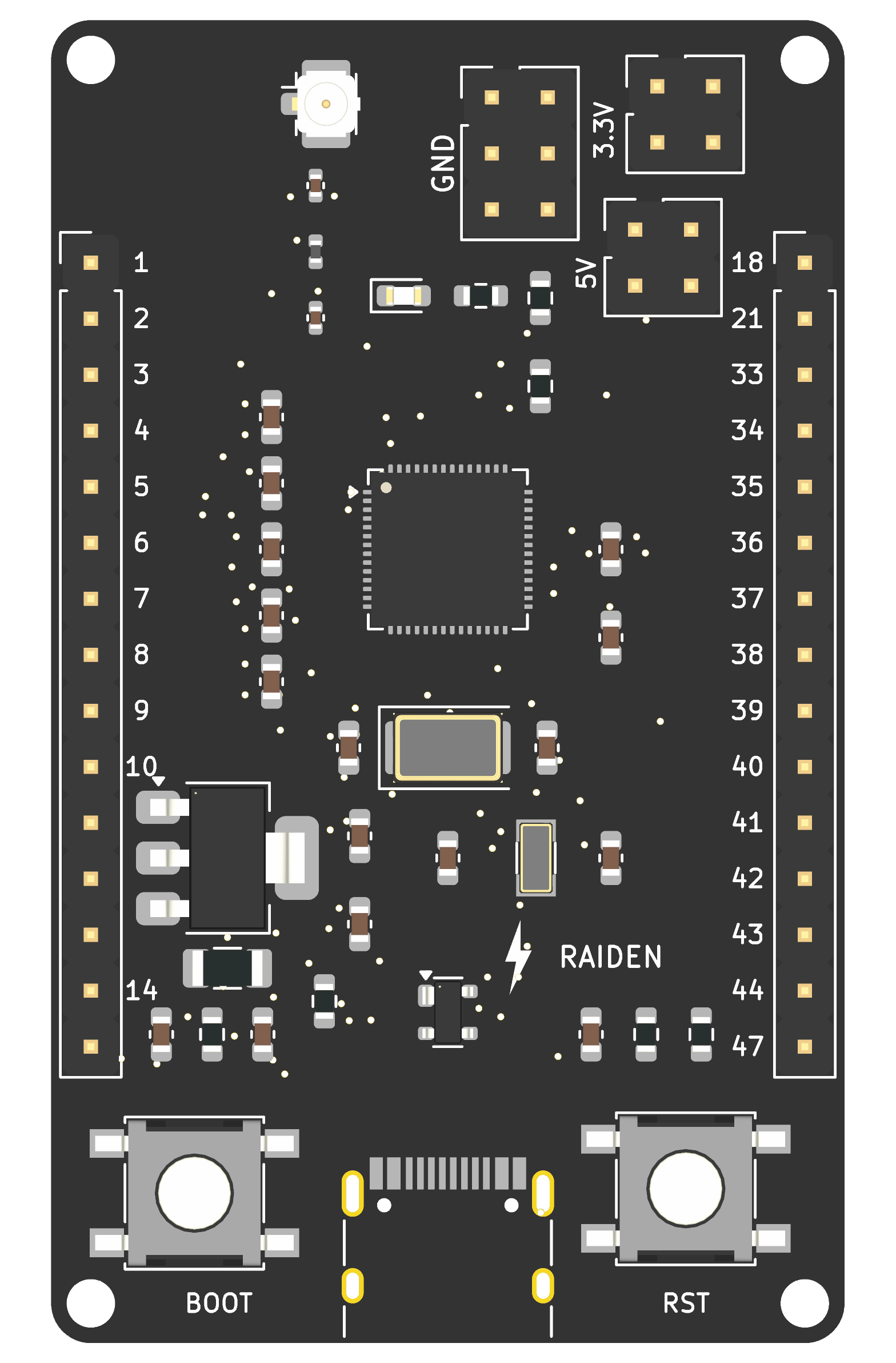 | 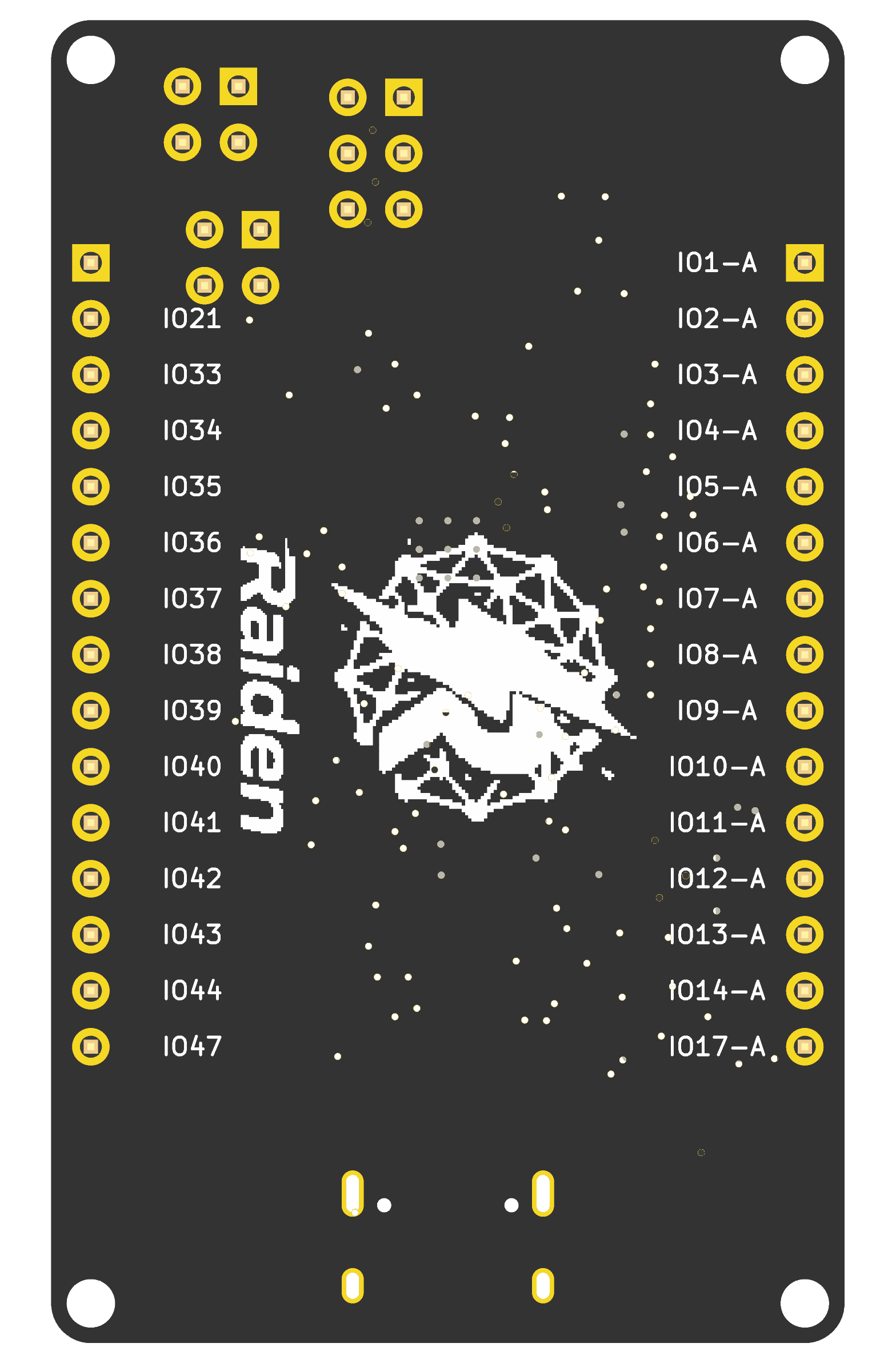 |
kicad-cli)hardware/ KiCad 9 project (schematic, PCB, project file)
fab/ Production package: Gerbers (4-layer), drill files,
BOM + CPL (JLCPCB format), pick-and-place, schematic PDF
images/ kicad-cli 3D rendersFull notes in fab/README.txt. Highlights:
Rev A — design complete and verification-clean; first fabrication run pending.
Hardware licensed under CERN-OHL-P v2 (LICENSE). Use it, modify it, build on it.
| Qty | Value | Footprint | References |
|---|---|---|---|
| 7 | 100nF | Capacitor_SMD:C_0603_1608Metric | C1, C2, C3, C4, C5, C15, C16 |
| 4 | 10k OHM | Resistor_SMD:R_0603_1608Metric | R1, R2, R3, R7 |
| 4 | MountingHole_M2 | MountingHole:MountingHole_2.2mm_M2 | H1, H2, H3, H4 |
| 2 | 10pF | Capacitor_SMD:C_0603_1608Metric | C9, C10 |
| 2 | 10uF | Capacitor_SMD:C_0603_1608Metric | C6, C7 |
| 2 | 1pF | Capacitor_SMD:C_0402_1005Metric | C17, C18 |
| 2 | 1uF | Capacitor_SMD:C_0603_1608Metric | C8, C13 |
| 2 | 22pF | Capacitor_SMD:C_0603_1608Metric | C11, C12 |
| 2 | 5.1k OHM | Resistor_SMD:R_0603_1608Metric | R4, R5 |
| 2 | Conn_01x15 | Connector_PinHeader_2.54mm:PinHeader_1x15_P2.54mm_Vertical | J1, J2 |
| 2 | Conn_02x02_Counter_Clockwise | Connector_PinHeader_2.54mm:PinHeader_2x02_P2.54mm_Vertical | J5, J6 |
| 2 | SW_Push | Button_Switch_SMD:SW_SPST_B3S-1000 | SW1, SW2 |
| 1 | 2.0nH | Inductor_SMD:L_0402_1005Metric | L1 |
| 1 | 32.768kHz | Crystal:Crystal_SMD_3215-2Pin_3.2x1.5mm | Y1 |
| 1 | 4.7uF | Capacitor_SMD:C_0603_1608Metric | C14 |
| 1 | 40MHz | Crystal:Crystal_SMD_5032-2Pin_5.0x3.2mm | Y2 |
| 1 | 470 OHM | Resistor_SMD:R_0603_1608Metric | R6 |
| 1 | AZ1117C-3.3 | Package_TO_SOT_SMD:SOT-223 | U2 |
| 1 | Antenna | Connector_Coaxial:U.FL_Hirose_U.FL-R-SMT-1_Vertical | ANT1 |
| 1 | Conn_02x03_Counter_Clockwise | Connector_PinHeader_2.54mm:PinHeader_2x03_P2.54mm_Vertical | J4 |
| 1 | ESP32-S3FN8 | Package_DFN_QFN:QFN-56-1EP_7x7mm_P0.4mm_EP4x4mm | U1 |
| 1 | PRTR5V0U2X | Package_TO_SOT_SMD:SOT-143 | D1 |
| 1 | PTC 750mA | Fuse:Fuse_1206_3216Metric | F1 |
| 1 | RED_LED | LED_SMD:LED_0603_1608Metric | D2 |
| 1 | USB_C_Receptacle_USB2.0_14P | Connector_USB:USB_C_Receptacle_HRO_TYPE-C-31-M-12 | P1 |
It measures 36 × 60 mm and has 4 copper layers, 1.6 mm thick.
46 parts, built around the ESP32-S3FN8 and PRTR5V0U2X. The full list of its parts is on this page, with links to each part's symbol and footprint where PCBKit's library has them.
From the RaidenTechnology/raiden-s01 repository on GitHub, at the commit this page was made from: the board is hardware/Raiden S0-1.kicad_pcb and its schematic hardware/Raiden S0-1.kicad_sch. PCBKit opens the board in the browser, with nothing to install.
Its repository publishes it under the CERN-OHL-P-2.0 licence: you may reuse it on that licence's terms (keep the author's notice, and for a copyleft licence share your changes alike).
CDFER/NIMRS-21Pin-Decoder
An open source 21-Pin DCC Decoder for model trains


JosueAGtz/ESP32-S3-Stick
ESP32-S3 is a dual-core XTensa LX7 MCU, capable of running at 240 MHz. Apart from its 512 KB of internal SRAM, it also comes with integrated 2.4 GHz, 802.11 b/g/n Wi-Fi and Bluetooth 5 (LE) connectivity that provides…

Mines-Rocketry-Club/flight-computers
Fully open source high power rocketry flight computers.

DLaxV-Community-Projects-Hub/Open-Shot-Clock
Build your own DIY Shot Clock

