2 layers19 × 14 mm
 Quil180/JuniorDesign
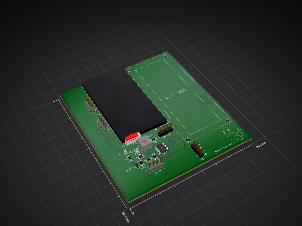
Main pcb is an open-source printed circuit board by Quil180, from the Quil180/JuniorDesign repository on GitHub. It is a 2-layer board of 88.8 × 99.1 mm with 20 parts on 30 nets, routed with 85 tracks and 5 vias.
It is built around the MSP430G2553IPW20R, 3362P-1-103LF and BS170FTA. It belongs with the MSP430 boards of this library.


| Qty | Value | Footprint | References |
|---|---|---|---|
| 3 | 1k | PCM_Resistor_SMD_AKL:R_1206_3216Metric | 1k, 1k, 1k |
| 3 | Conn_01x04_Socket | footprints:CON4_1X4_TU_SSQ | 3.3V1, 5V1, Sensor1 |
| 2 | 10k | PCM_Resistor_SMD_AKL:R_1206_3216Metric | 10k, 10k |
| 2 | Conn_01x04_Pin | Connector_PinHeader_2.54mm:PinHeader_1x04_P2.54mm_Vertical | LCD, Programmer |
| 2 | LED_0805_Red | PCM_LED_SMD_AKL:LED_0805_2012Metric | LED_MOSFET1, LED_PWM |
| 1 | 09.03201.02 | footprints:09.03201_EAO | SW |
| 1 | 2462 | footprints:2462_KEY | Battery1 |
| 1 | 3362P-1-103LF | footprints:POT_3362P | Potent. |
| 1 | 510 | PCM_Resistor_SMD_AKL:R_1206_3216Metric | 510 |
| 1 | BS170FTA | footprints:SOT-23_DIO | MOSFET |
| 1 | MSP430G2553IPW20R | footprints:PW20 | U1 |
| 1 | ~ | jDPCB:JHD-162A | lcd_jdpcb1 |
The 19 most common of 20 parts.

Severson-Group/AMDC-Hardware
Circuit board designs for controlling advanced motor systems

slemanz/chronolog
STM32-based temperature data logger with RTC, NOR flash storage, LCD and Wi-Fi. Hardware and firmware.


justharihere/PWM_Modulator
This is an experimental PWM Modulator I developed while experimenting with NE555 timer ICs, datasheets, and learning PCB fab.


NarekKalikian/Microcontroller-Projects
A variety of microcontroller projects combining principles of computer engineering, electrical engineering, circuit design, and programming.
It measures 88.8 × 99.1 mm and has 2 copper layers, 1.6 mm thick.
20 parts, built around the MSP430G2553IPW20R, 3362P-1-103LF and BS170FTA. The full list of its parts is on this page, with links to each part's symbol and footprint where PCBKit's library has them.
From the Quil180/JuniorDesign repository on GitHub, at the commit this page was made from: the board is KicadProjects/main_pcb/main_pcb.kicad_pcb and its schematic KicadProjects/main_pcb/main_pcb.kicad_sch. PCBKit opens the board in the browser, with nothing to install.
Its repository states no licence, so its author keeps all rights: ask Quil180 before reusing the design.