
2 layers160 × 51 mm
Console a
jmcpheron/pico-quorum
Several people, several keys, one Safe. Hardware approvals for Safe multisig wallets.
38 partsMIT
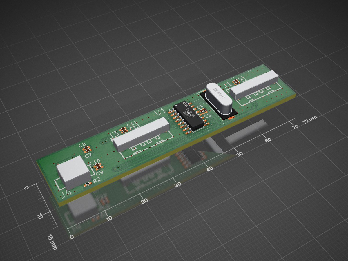
Customized USB 2.0 Hub for Rainy 75 RT. Goes onto the Type C Port.
Hub is an open-source printed circuit board by PythonOrC, from the PythonOrC/USB-HUB-Keyboard repository on GitHub. It is a 2-layer board of 72 × 15 mm with 18 parts on 30 nets, routed with 279 tracks and 106 vias.
It is built around the SL2.1A, 918-118A2021Y40002 and TYPEC-303-ACP16. Its parts include 10 capacitors, 4 connectors, 2 resistors, 1 IC and 1 crystal.


| Qty | Value | Footprint | References |
|---|---|---|---|
| 6 | 10 uF | Capacitor_SMD:C_0402_1005Metric_Pad0.74x0.62mm_HandSolder | C1, C3, C4, C7, C9, C11 |
| 4 | 0.1 uF | Capacitor_SMD:C_0402_1005Metric_Pad0.74x0.62mm_HandSolder | C2, C8, C10, C12 |
| 2 | 10.0 180° ZCJB-HJ | custom-components:USB-A-FEMALE | J1, J3 |
| 2 | 5.1k | Resistor_SMD:R_0402_1005Metric_Pad0.72x0.64mm_HandSolder | R1, R2 |
| 1 | 12 MHz | Crystal:Crystal_SMD_HC49-SD | X1 |
| 1 | 918-118A2021Y40002 | custom-components:TYPE-C-SMD-MALE | J2 |
| 1 | SL2.1A | custom-components:SOP-16_L10.0-W3.9-P1.27-LS6.0-BL | U1 |
| 1 | TYPEC-303-ACP16 | custom-components:USB-C-SMD_TYPEC-303-ACP16 | J4 |
It measures 72 × 15 mm and has 2 copper layers, 1.6 mm thick.
18 parts, built around the SL2.1A, 918-118A2021Y40002 and TYPEC-303-ACP16. The full list of its parts is on this page, with links to each part's symbol and footprint where PCBKit's library has them.
From the PythonOrC/USB-HUB-Keyboard repository on GitHub, at the commit this page was made from: the board is source/hub/hub.kicad_pcb and its schematic source/hub/hub.kicad_sch. PCBKit opens the board in the browser, with nothing to install.
Its repository states no licence, so its author keeps all rights: ask PythonOrC before reusing the design.
jmcpheron/pico-quorum
Several people, several keys, one Safe. Hardware approvals for Safe multisig wallets.


Arrow-air/project-caribou
Project Caribou documentation, designs, and project artifacts.

mrspieb/HW-FanControl
Everything required to build the PCB and case of the ventilation fan controller

OpenIPC/hardware
A collection of hardware developments by the OpenIPC team

Pwnsat/PWNCUBE
PWNCUBE v1.0 is a Cubesat hardware based platform for aerospace cybersecurity research

thatoddmailbox/kvm-base
The main board for the open-source HDMI KVM switch I built.
