

2 layers150 × 100 mm
Dual current mirror
Polymorphic548/EDC_project
This directory contains the KiCad implementation of the diode-compensated current mirror: a reusable circuit and a 150 x 100 mm panel containing two isolated copies.
36 partsMIT

 Polymorphic548/EDC_project
This directory contains the KiCad implementation of the diode-compensated current mirror: a reusable circuit and a 150 x 100 mm panel containing two isolated copies.
Current mirror is an open-source printed circuit board by Polymorphic548, from the Polymorphic548/EDC_project repository on GitHub, published under the MIT licence. It is a 2-layer board of 78 × 67 mm with 18 parts on 12 nets, routed with 50 tracks and 0 vias.
It is built around the BZX55C5V1. Its parts include 7 resistors, 4 diodes, 4 connectors, 2 transistors and 1 capacitor.
This directory contains the KiCad implementation of the diode-compensated current mirror: a reusable circuit and a 150 x 100 mm panel containing two isolated copies. See the project overview for component values and measurement instructions.
| Project | Purpose | Board size |
|---|---|---|
| dual_current_mirror.kicad_pro | Complete panel for fabrication | 150 x 100 mm |
| current_mirror.kicad_pro | Reusable single circuit | 78 x 67 mm |
Open with KiCad 10.0.7 or later. Open the PCB in PCB Editor and press Alt+3 for 3D. Both projects use Project.pretty through the supplied fp-lib-table. Reopen files from disk after external edits to avoid saving an older editor copy over them.
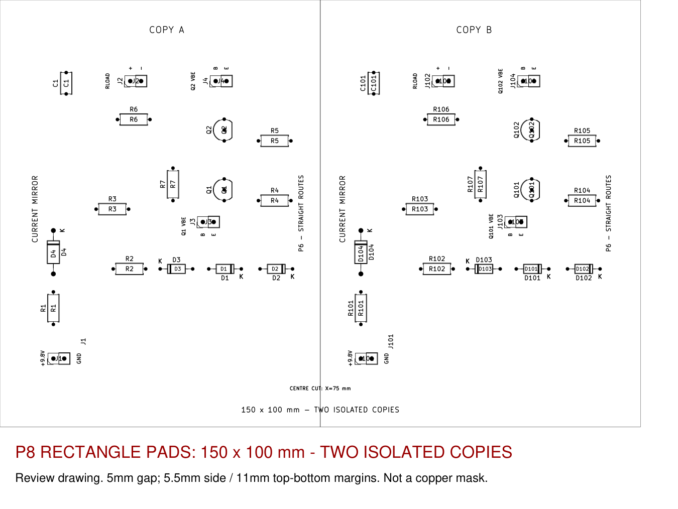
Assembly PDF | Copper review | Schematic PDF
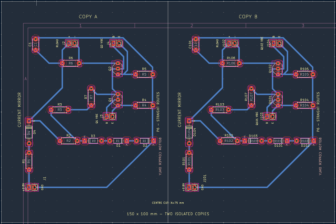
The supplied screenshot shows the current placement and routing before the rectangular-pad update. The generated previews show the current pad outlines.
| Parameter | Specification |
|---|---|
| Physical copper / thickness | Single-sided B.Cu / 1.7 mm |
| Tracks | 0.6 mm; horizontal, vertical and 45 degrees sections |
| Configured minimum different-net clearance | 0.8 mm |
| Vias / jumpers / pours | None |
| Footprints / nets | 36 / 24 |
| Pad shapes | 36 rectangular, 40 circular |
| Holes | 56 x 0.8 mm; 16 x 1.0 mm; 4 x 1.1 mm |
Each unit is rotated 90 degrees, occupying 67 x 78 mm. Copy A's unit rectangle spans x=5.5-72.5 mm, y=11-89 mm; copy B spans x=77.5-144.5 mm, y=11-89 mm. The unit rectangles have a 5 mm gap.
Copy B adds 100 to the references: Q1 -> Q101, J1 -> J101, etc. All A/B nets are separate, including ground. Shared external supplies or instruments can connect them externally.
Only the outer boundary is on Edge.Cuts. The centre separation line is on User.1 and exports separately. Through-hole pads appear on both copper layers in KiCad's data model; all routing and fabrication copper artwork are B.Cu.
All eight connectors are 1x2 male headers, 2.54 mm pitch. Use female jumper leads for power and instruments.
| Function | Copy A / B | Pin 1 | Pin 2 |
|---|---|---|---|
| 9.8 V power | J1 / J101 | VIN | GND |
| Load voltage | J2 / J102 | VCC | OUT |
| First transistor VBE | J3 / J103 | BASE | E1 |
| Second transistor VBE | J4 / J104 | BASE | E2 |
Use DC volts with red on pin 1 and black on pin 2. Emitters are separate nodes above their 22 ohm resistors. Do not fit shorting caps.
In the single-unit orientation, transistor pads are 1.7 x 2.4 mm with 0.8 mm holes; header pads are 2.4 x 1.7 mm with 1.0 mm holes. Both have 2.54 mm pitch and a 0.84 mm adjacent-pad gap. Panel rotation swaps the X/Y dimensions.
All transistor and header pads are rectangular. Identify pins by numbering and assembly labels, not pad shape. Transistor numbering is 1=E, 2=B, 3=C; check the actual manufacturer's pinout. Confirm lead forming, resistor pitch of 7.62 mm and C1's assumed 5 mm lead spacing before fabrication.
Panel BOM | Panel component/net data | Unit BOM
Use dual_panel_machine_files.zip. The separately named dual_panel_coppercam_rectangles.zip contains identical files for the fresh import check.
| File | Import as |
|---|---|
dual_current_mirror-B_Cu.gbr | Copper to retain |
dual_current_mirror.drl | Excellon drilling data |
dual_current_mirror-Edge_Cuts.gbr | Optional outer outline |
dual_current_mirror-Centre_Cut.gbr | Optional centreline separation cut |
All files use millimetres, absolute coordinates and a shared unmirrored origin. Apply machine-side positioning or mirroring consistently to copper, drilling and cutting. No front-copper file is required. These files are CAM inputs; the operator generates executable machine output.
For CopperCAM:
The export contains only standard circle/rectangle pad apertures, without oval pads, rounded rectangles, aperture macros or filled pad regions. The rectangular-pad version still requires import confirmation in the lab's CopperCAM installation.
The centre-cut file contains one straight line at x=75 mm, y=0-100 mm in board coordinates. Import it as a separate centreline cutting operation, preserving alignment with the copper. It is not a closed outline or copper artwork.
centre_cut_setup.json records the SRM-20, 1.7 mm board, 0.8 mm cutter diameter and maximum 0.4 mm pass depth. Nominal planning depths to board bottom are 0.4, 0.8, 1.2, 1.6 and 1.7 mm.
No executable RML/G-code or tabs are included. The operator must confirm feeds, spindle speed, safe Z, Z-zero, cutter type/usable length, holding, breakthrough allowance and output format. Secure both halves over a suitable sacrificial board and complete isolation and drilling before separation. A centred 0.8 mm kerf leaves nominal 74.6 x 100 mm halves without outer trimming.
Unmirrored 1:1 PDF | Mirrored 1:1 PDF
These contain B.Cu only; black denotes copper to keep. Confirm transfer orientation and exposure polarity with the lab. Print at Actual Size / 100%, measure the 50 mm calibration line and transfer only the board area. Review drawings are not masks. See printing instructions.
Recorded native checks report zero ERC/DRC violations, zero unconnected items and zero schematic-parity issues under the configured rules. Independent audits cover component values, netlist-to-pad agreement, header roles, unique identifiers, isolation, clearances and all 76 pad/drill locations.
| Record | Scope |
|---|---|
| Panel audit | Dimensions, isolated nets and component mapping |
| Panel ERC / DRC | Native KiCad checks |
| Source connectivity | LTspice topology comparison |
| Solder clearance | Pad gaps and annular copper |
| Pad audit | Rectangular transistor pads and Gerber apertures |
| Export verification | Copper/drill geometry and cutting files |
| Panel hashes | Design and print-artifact integrity |
The reports establish saved-file consistency, not machining or electrical performance. Original LTspice files are preserved. The PCB uses fixed nominal 120 ohm resistors; the original source used RV=117.6 ohm. Earlier revision reports and trimmer templates are historical records.
The scripts include generators, routing, exports and checks. KiCad's bundled Python supplies pcbnew; PNG preview rendering uses regular Python with PyMuPDF. Some source checks also read installed LTspice symbols.
Treat the saved CAD files as the handoff design. Back up manual edits before running generators or the router: they rebuild geometry and may replace the saved placement or routing. After CAD changes, regenerate the relevant netlists, ERC/DRC/parity reports, audits, previews and manufacturing exports before packaging a new ZIP.
export_machine_files.ps1 exports machine files; check_machine_files.py compares them with the board and writes verification/checksum records. Package those checked files together. Documentation-only edits do not require regeneration of manufacturing artifacts.
| Qty | Value | Footprint | References |
|---|---|---|---|
| 1 | 1.33n / >=25V | Project:C1_ETCH | C1 |
| 1 | 120R (117.6R measured) | Project:R7_ETCH | R7 |
| 1 | 1N4007 | Project:D4_ETCH | D4 |
| 1 | 1N4148 | Project:D2_ETCH | D2 |
| 1 | 1N4148 | Project:D1_ETCH | D1 |
| 1 | 1R (LT F1) | Project:R1_ETCH | R1 |
| 1 | 1k (LT R1a) | Project:R3_ETCH | R3 |
| 1 | 1k (LT Rload) | Project:R6_ETCH | R6 |
| 1 | 22R (LT Re1) | Project:R4_ETCH | R4 |
| 1 | 22R (LT Re2) | Project:R5_ETCH | R5 |
| 1 | 2N3904 | Project:Q1_ETCH | Q1 |
| 1 | 2N3904 | Project:Q2_ETCH | Q2 |
| 1 | 662R (LT Rs) | Project:R2_ETCH | R2 |
| 1 | 9.8V INPUT | Project:J1_ETCH | J1 |
| 1 | BZX55C5V1 | Project:D3_ETCH | D3 |
| 1 | Q1 BASE-EMITTER | Project:J3_ETCH | J3 |
| 1 | Q2 BASE-EMITTER | Project:J4_ETCH | J4 |
| 1 | RLOAD VOLTAGE | Project:J2_ETCH | J2 |
It measures 78 × 67 mm and has 2 copper layers, 1.7 mm thick.
18 parts, built around the BZX55C5V1. The full list of its parts is on this page, with links to each part's symbol and footprint where PCBKit's library has them.
From the Polymorphic548/EDC_project repository on GitHub, at the commit this page was made from: the board is PCB layout/current_mirror.kicad_pcb and its schematic PCB layout/current_mirror.kicad_sch. PCBKit opens the board in the browser, with nothing to install.
Its repository publishes it under the MIT licence: you may reuse it on that licence's terms (keep the author's notice, and for a copyleft licence share your changes alike).
Polymorphic548/EDC_project
This directory contains the KiCad implementation of the diode-compensated current mirror: a reusable circuit and a 150 x 100 mm panel containing two isolated copies.

4106677/pramac-pmd5050s-autostart
Автозапуск дизель-генератора Pramac PMD5050S на ESP32 (ESPHome) + Home Assistant


MadsRudolph/62768-energy-system
Team project for 62768 Electrical Energy Systems (DTU, June 2026, 3-week course). We design and build a complete electrical energy system per the course requirement spec (Kravspecifikation), from idea to a working…


VoronDesign/Voron-Hardware
Cool Hardware designed by the Voron Design group