4 layers100 × 100 mm

 plan44/p44ttngw-hardware4
KiCAD files for TTN LoRA gateway based on RAK831 and Omega2S
P44ttngw is an open-source printed circuit board by plan44, from the plan44/p44ttngw-hardware repository on GitHub. It is a 2-layer board of 80 × 51.4 mm with 78 parts on 92 nets, routed with 582 tracks and 18 vias.
It is built around the R-78C5.0-1.0 and STPS1L30A. Its parts include 15 resistors, 13 capacitors, 7 diodes, 7 connectors and 3 ICs. It belongs with the radio and wireless boards of this library.


This repository contains the KiCAD CAE files for a RAK831 + Omega2S based TTN LoRa gateway. This PCB can be sandwitched with a RAK831 LoRa concentrator board and fits into a 909060mm IP65 watertight Hammond 1554EGY enclosure.
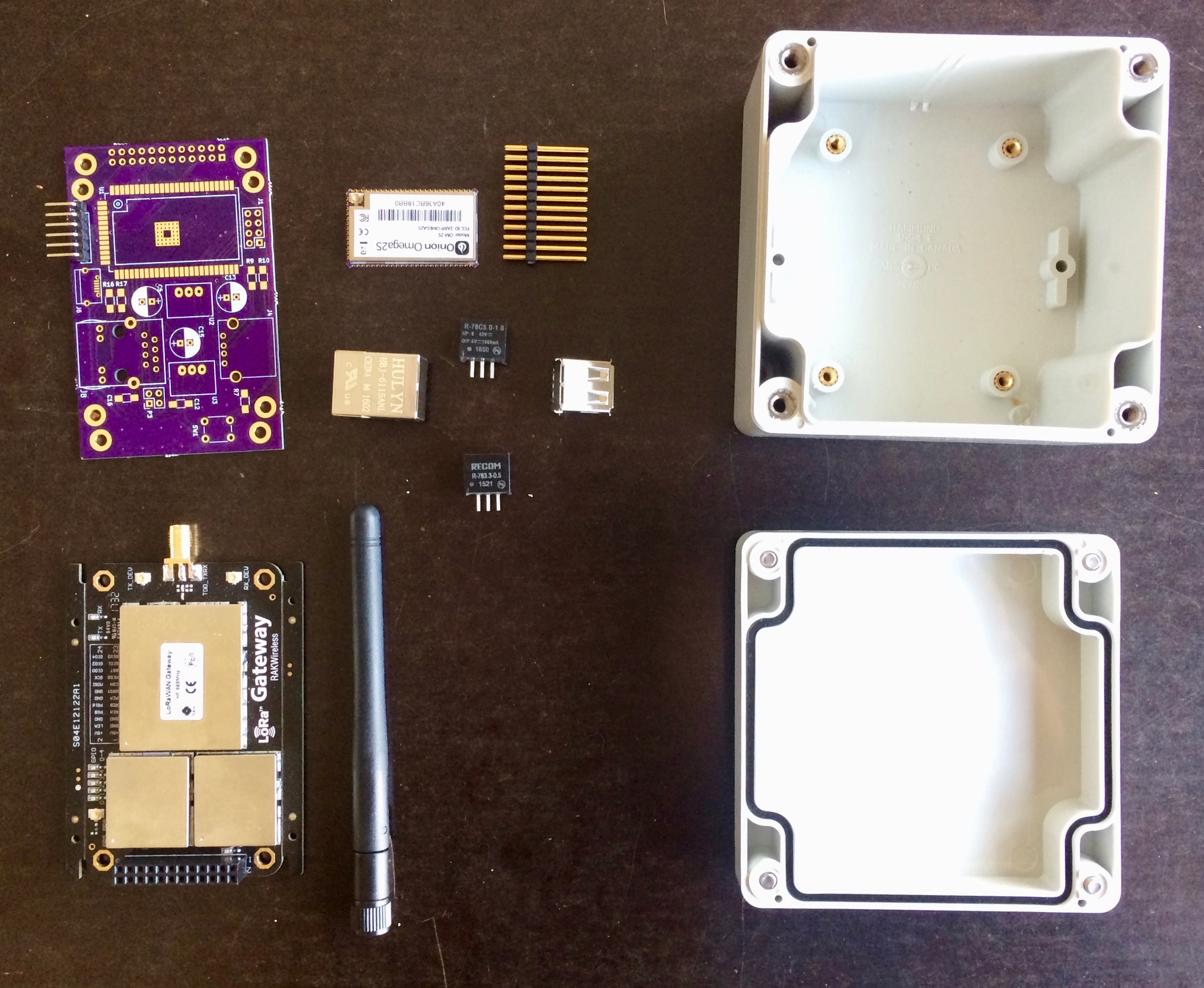
The firmware for the project (a customized LEDE build) is contained in the plan of the plan44-feed LEDE feed repository in the p44ttngw-config package, see README there about how to build the firmware image from scratch.
The resulting image can be installed on a Omega2 or Omega2S and will start to act as a TTN gateway after powerup.
You can order the board (actually, 3 of them) directly from OSH Park or of course use the KiCAD file to produce gerbers for any other PCB fabber.
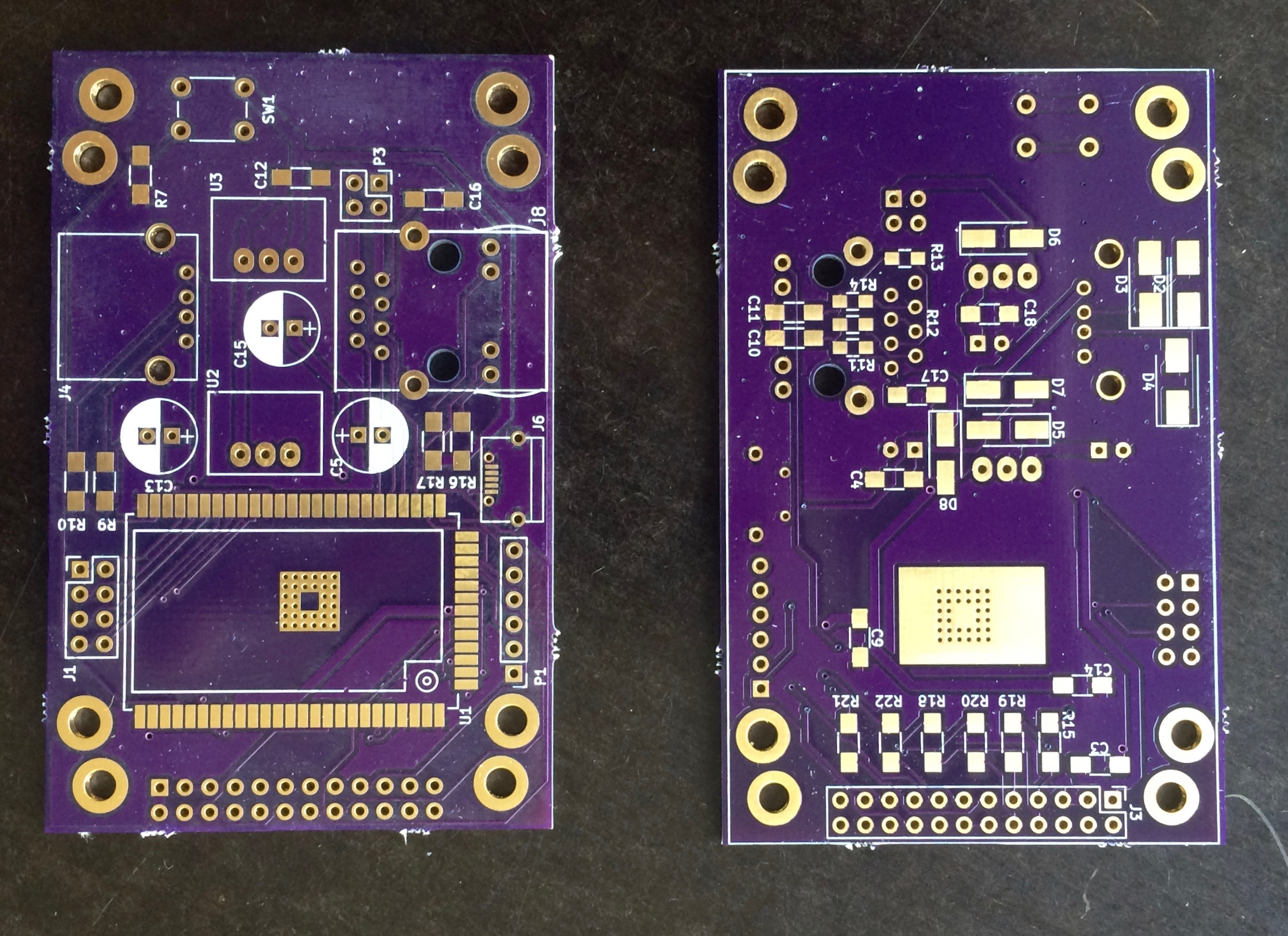 OSHPark PCBs
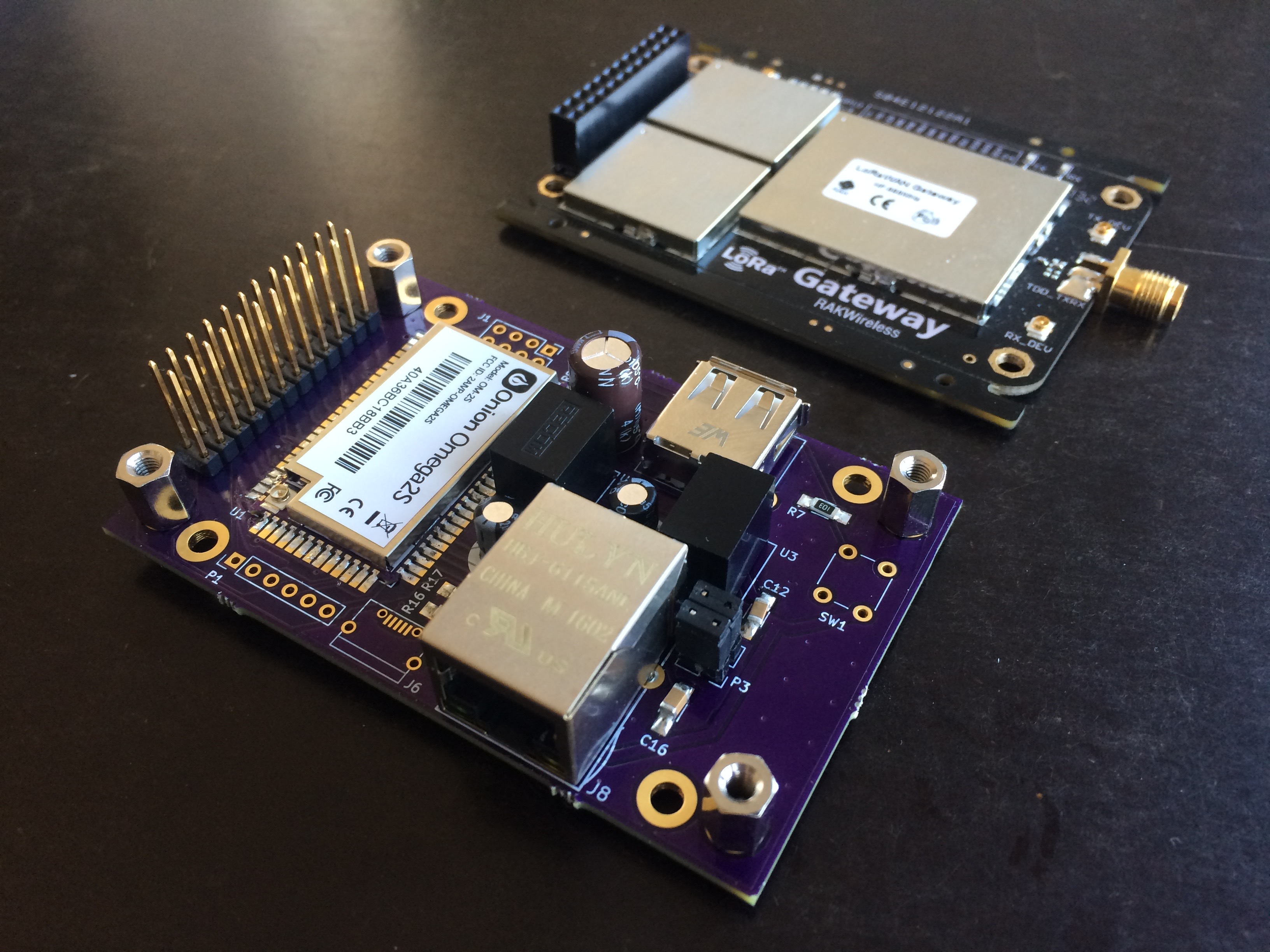 The soldered board (mostly SMT, I found with a bit of practice 1206 sized Rs and Cs are quicker to solder than THT, and the parts are much cheaper).
 Everything in the box. The plastic PCB guides inside the case need to be cut away, and the hole for the antenna should be precise, so it can be made watertight with thin rubber sealing rings inside and outside.
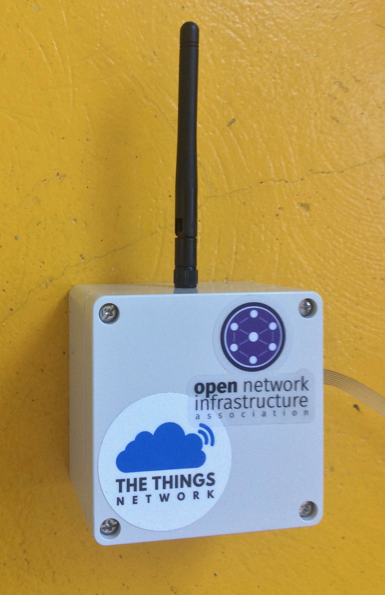
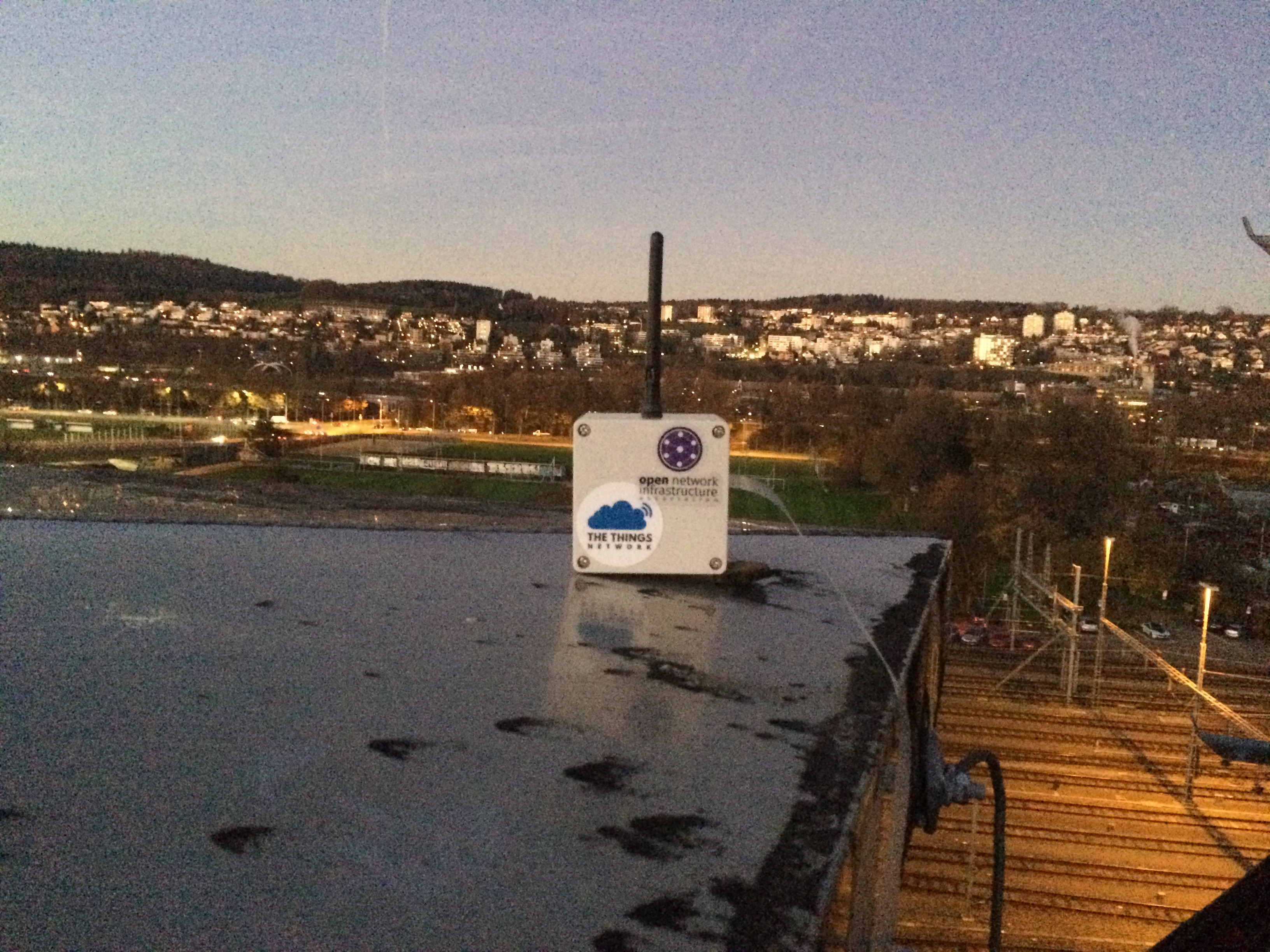 First tests on the roof where it will get permanently mounted, but eventually with a real ethernet cable grommet (and probably a better antenna - more experienced TTN forum users told me the RAK831 antenna is not really good).
| Qty | Value | Footprint | References |
|---|---|---|---|
| 28 | Stitching-VIA-0.6mm | plan44:Stitching-VIA-0.6mm | VIA, VIA, VIA, VIA, VIA, VIA, VIA, VIA, VIA, VIA, VIA, VIA, VIA, VIA, VIA, VIA +12 |
| 9 | 100nF | Capacitors_SMD:C_1206_HandSoldering | C3, C4, C9, C10, C11, C12, C14, C17, C18 |
| 6 | 0R | Resistors_SMD:R_1206_HandSoldering | R15, R18, R19, R20, R21, R22 |
| 4 | 49.9_1% | Resistors_SMD:R_0805_HandSoldering | R11, R12, R13, R14 |
| 4 | CONN_01X01 | Mounting_Holes:MountingHole_3.2mm_M3_DIN965_Pad | MH1, MH2, MH3, MH4 |
| 4 | STPS1L30A | Diodes_SMD:D_SMA_Handsoldering | D5, D6, D7, D8 |
| 3 | DO-214AA | Diodes_SMD:D_SMB_Handsoldering | D2, D3, D4 |
| 2 | 1k | Resistors_SMD:R_1206_HandSoldering | R16, R17 |
| 2 | 22uF 25V | Capacitors_ThroughHole:CP_Radial_D7.5mm_P2.50mm | C5, C15 |
| 2 | 47R | Resistors_SMD:R_1206_HandSoldering | R9, R10 |
| 1 | 10k | Resistors_SMD:R_1206_HandSoldering | R7 |
| 1 | 10uF 50VDC | Capacitors_ThroughHole:CP_Radial_D7.5mm_P2.50mm | C13 |
| 1 | 1uF | Capacitors_SMD:C_1206_HandSoldering | C16 |
| 1 | CONN_02X02 | Pin_Headers:Pin_Header_Straight_2x02_Pitch2.54mm | P3 |
| 1 | CONN_02X04 | Pin_Headers:Pin_Header_Straight_2x04_Pitch2.54mm | J1 |
| 1 | FDI_Cable | Pin_Headers:Pin_Header_Straight_1x06_Pitch2.54mm | P1 |
| 1 | HLJ-6115ANL | plan44:HLJ-6115ANL | J8 |
| 1 | ONION-OMEGA2S | plan44:ONION-OMEGA2S | U1 |
| 1 | Omron PB | Buttons_Switches_ThroughHole:SW_PUSH_6mm_h4.3mm | SW1 |
| 1 | R-78C5.0-1.0 | plan44:Recom-R78Cxx | U2 |
| 1 | RAK831 | plan44:RAK831 | J3 |
| 1 | R_783.3-0.5 | plan44:Recom-R78Cxx | U3 |
| 1 | USB_A | Connect:USB_A | J4 |
| 1 | USB_Micro_AB | plan44:USB_Micro-B-SMD | J6 |


oxfordfish/STM32G0F6Px-ROC
A reverse osmosis controller system designed around STM32.

chapppy/Board-for-Relay-Card
Design of schematic and PCB for Relay Card control over USB and CAN based on STM32

MateuszKozaczek/eink-NFC-PCB
This is PCB project of smart tag for master's degree diploma project

radioelf/nano_Drone_ESP32
Small drone with ESP32 to experiment with this https://github.com/rtlopez/esp-fc

It measures 80 × 51.4 mm and has 2 copper layers, 1.6 mm thick.
78 parts, built around the R-78C5.0-1.0 and STPS1L30A. The full list of its parts is on this page, with links to each part's symbol and footprint where PCBKit's library has them.
From the plan44/p44ttngw-hardware repository on GitHub, at the commit this page was made from: the board is p44ttngw-kicad/p44ttngw.kicad_pcb. PCBKit opens the board in the browser, with nothing to install.
Its repository states no licence, so its author keeps all rights: ask plan44 before reusing the design.