Skip to the content
2 layers112.1 × 88.2 mmPDB, the printed circuit board in 3D

PiElectrical Work and Documentation

Size
112.1 × 88.2 mm
Copper layers
2
Thickness
1.6 mm
Parts
104
Nets
85
Pads
325
Tracks, vias
733, 118
Pours
5
Routed
Yes
KiCad
KiCad 10.0 (file 20260206)
Created
20 Sep 2016
Updated
1 Oct 2026

Overview

PDB is an open-source printed circuit board by pioneers, from the pioneers/PiElectrical repository on GitHub. It is a 2-layer board of 112.1 × 88.2 mm with 104 parts on 85 nets, routed with 733 tracks and 118 vias.

It is built around the ATMEGA32U4-MU, LM66100DCK and USBLC6-2SC6, with the MMBT3906 and BSS84 among its other parts. Its parts include 37 resistors, 14 capacitors, 11 transistors, 7 diodes and 4 ICs. It belongs with the AVR (ATmega, ATtiny) boards of this library.

Main components

5

README

README.md

PiElectrical

This is the working repo for PiElectrical teams

  1. ToDo
  2. Repo Structure
  3. Setup
  4. Work Flow
  5. How to Create a Gerber
  6. Docu Packets
  7. FAQ
  8. Useful Links
  9. Standards

ToDo:

  • The stuff in PDB-Y16
  • Convert motor controller design to KiCad
  • Add and test current regulation for motor controller
  • Talk to runtime and potentially use cheaper MCU for motor controller

Back to Top

Repo Structure:

Boards: Contains all necessary information about each board, including KiCad (and old Eagle) files, arduino test files, and board specific documentation.

Bootloaders: Contains the files necessary to burn the bootloader for boards identifying as Leonardo (Atmega32u4).

Documentation: All docu packets and scripts. Fragile! Do not touch!

Production_Files: Finalized gerbs and other necessary production files (BOM, CPL, etc...) sent out for fabrication.

Images: Place all your images in here to enhance your READMEs.

Libraries: Necessary KiCad files to work on PiElectrical

ToDo is on the README to keep things easier to see at first glance. GitHub issues tracker can be used as well.

Back to Top

Setup

When you see an arrow like this... (click me) ...it indicates an expandable section. We usually include images in here as a better reference for you to follow along.

Initial Setup of PiElectrical repo on your computer

  1. Copy the URL for pioneers/PiElectrical to your clipboard: (Or here: https://github.com/pioneers/PiElectrical.git)
  2. In Terminal (Mac, GNU/Linux) or Git Bash (windows), navigate to your working directory (the directory that you want to keep PiElectrical in.)
  3. Clone PiElectrical by running this command: git clone https://github.com/pioneers/PiElectrical.git

Installation of KiCad on your computer

  1. Download the latest version of KiCad here: https://www.kicad.org/download/
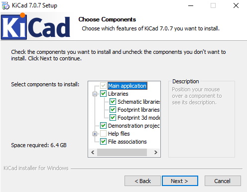
  2. Run installer. Use all default settings on installer. (Click to see default settings)

Setting up KiCad

  1. Open KiCad.
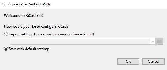
  2. Depending on whether you've used KiCad before, select the appropriate option on the pop-up. (Default settings if you're new to KiCad).
Adding Symbols
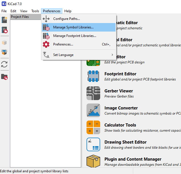
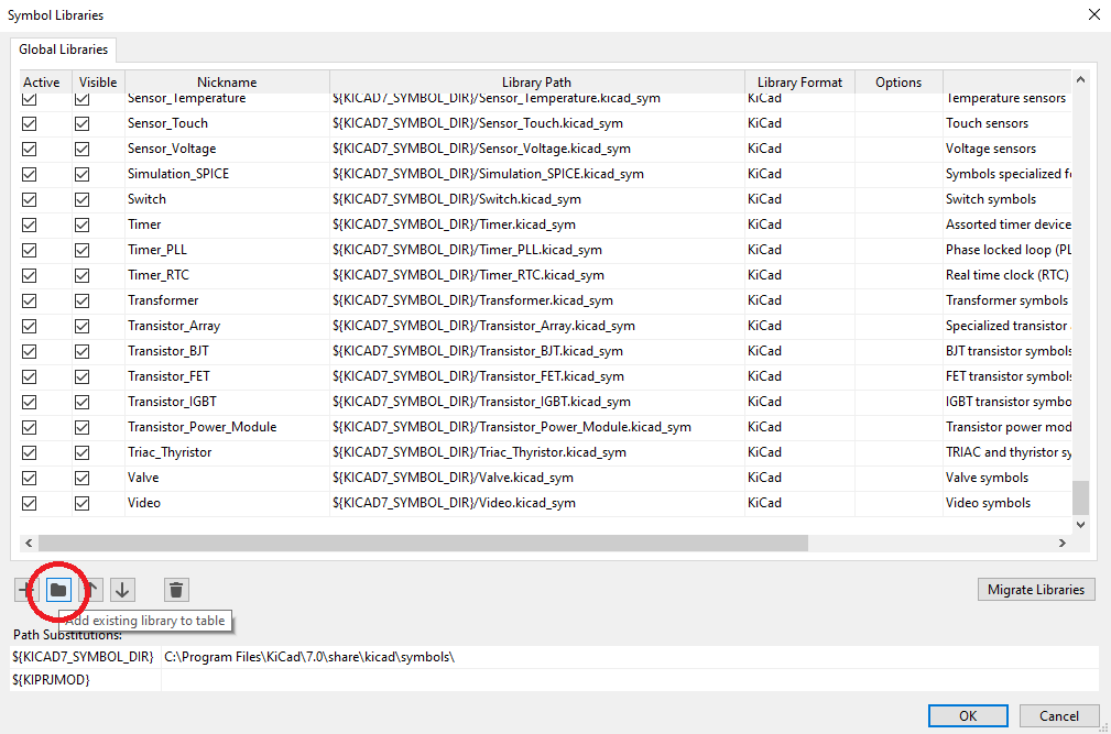
  1. Go to the Preferences tab, and select Manage Symbol Libraries...
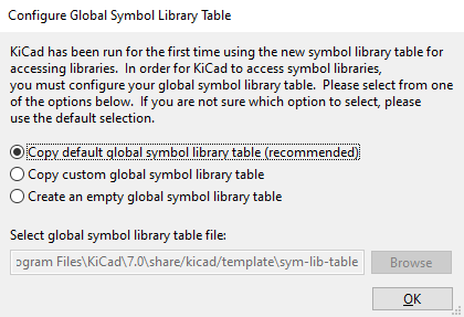
  2. If this is your first time using KiCad, it will prompt you to configure the Global Symbol Library. It is highly recommended that you select "Copy default global symbol library table".
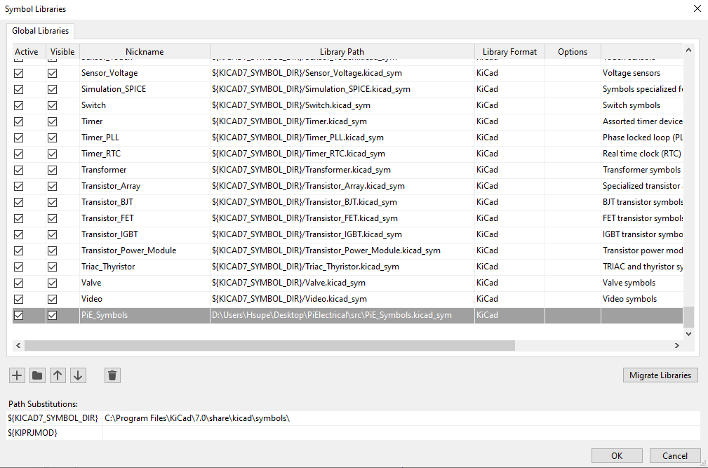
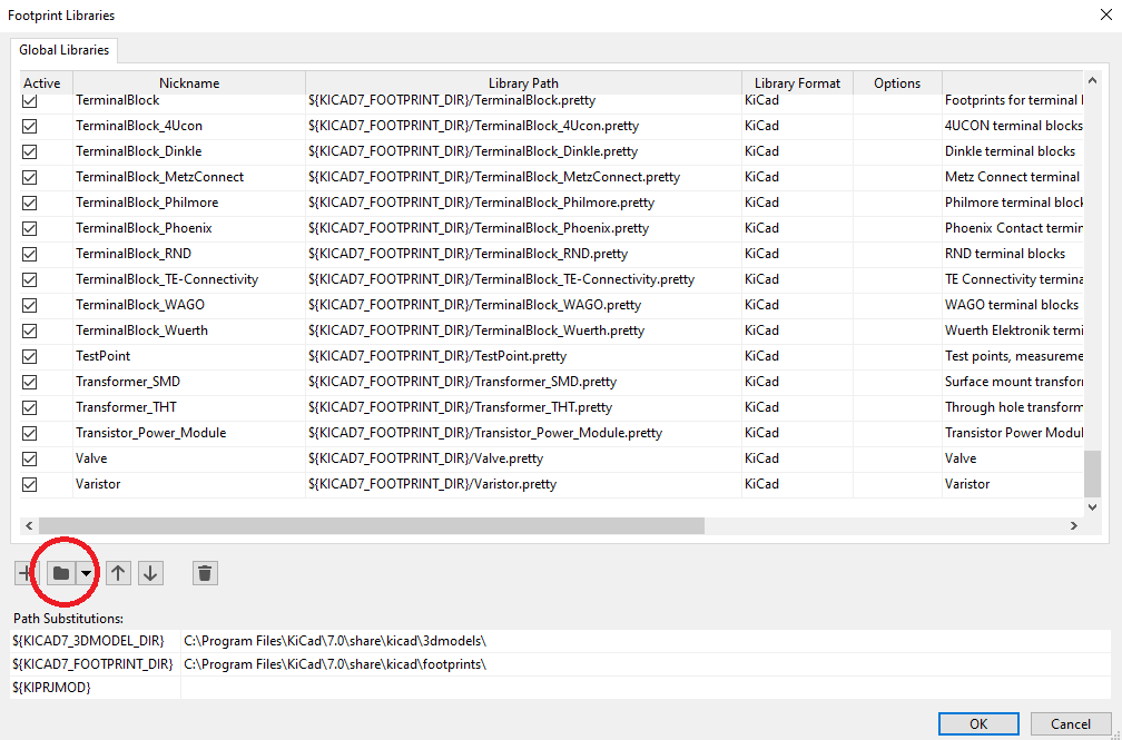
  3. Select the folder icon near the bottom left and navigate to the PiE_Symbols.kicad_sym file in the src folder.
  4. You should now see the PiE_Symbols in your Symbol Libraries. Make sure the "active" box is checked, and click "OK".
Adding Footprints
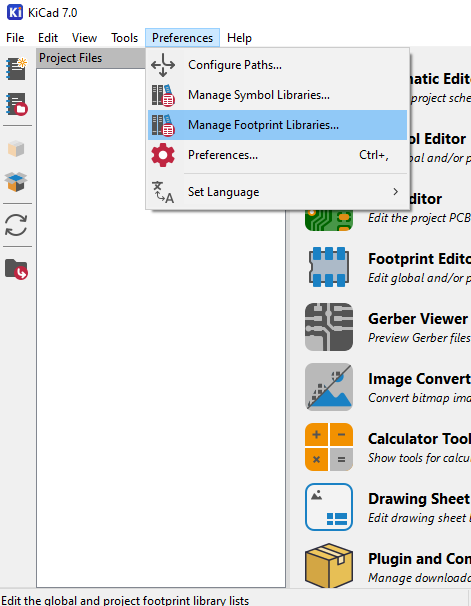
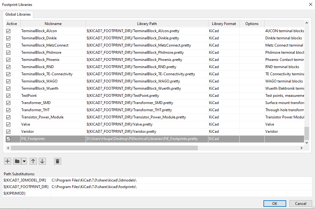
  1. Go to the Preferences tab, and select Manage Footprint Libraries...
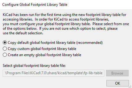
  2. If this is your first time using KiCad, it will prompt you to configure the Global Footprint Library. It is highly recommended that you select "Copy default global footprint library table".
  3. Select the folder icon near the bottom left and navigate to the PiE_Footprints.pretty file in the src folder.
  4. You should now see the PiE_Footprints in your Footprint Libraries. Make sure the "active" box is checked, and click "OK".

Note that this setup instruction is based on KiCad 7.0.7, but it should still work for other versions.

Back to Top

Work Flow

Protocol when working on KiCad files

The revision number should be REV <year><revision>. E.g. REV 16A for year 16 revision A.

If you are not quite familiar with git, see Useful Links for the PiE Github tutorial

WARNING: Do not modify PiE_Symbols.kicad_sym or PiE_Footprints.pretty without discussing it with PMs.

Steps when working on KiCad files:

  1. In Terminal (mac, GNU/Linux) or GitBash (windows), navigate to your working directory (wherever you have PiElectrical).
  2. Make sure your working directory is clean: git status
  3. If you haven't started your sub project: git checkout -b YOURNAME-SUBPROJECT
  4. YOUR_NAME/SUBPROJECT is now the name of your branch
  5. Do your work in KiCad.
  6. Once you are at a good stopping point in your KiCad work, commit your progress:
    1. git add path/to/your/file
    2. git commit -m "Make your commit message short and with this format"
    3. NOTE: Commiting is like saving your file, but for all of PiE as well as your personal computer. And just like saving, Commit Early & Commit Often!
  7. Repeat Steps 5 and 6 until you are finished with your EAGLE work.
  8. Once you have made your last commit, push your files to the PiElectrical github repo: git push origin YOUR_BRANCH
    • If you get a merge conflict, contact the PMs for help.
  9. If completely done, submit a Pull Request

Commit Message Format Conventions

  • Present Tense ("Reroute power traces on team flag", not "Rerouted power traces on team flag")
  • No period at the end: ("Reroute power traces on team flag", not "Reroute power traces on team flag.")
  • Keep your message length to about one sentence.

Merge Conflicts: What should I do?

Don't try to fix it yourself: Eagle files are finicky and you might break all your work!

Ask someone who knows how to deal with this, i.e. your PM or something

Back to Top

Generating Fabrication Outputs

  1. Make sure you run the Electrical Rules Check (ERC) in the schematic and the Design Rules Checker (DRC) in the layout, and have no red errors. Feel free to ask PMs if you have any questions.

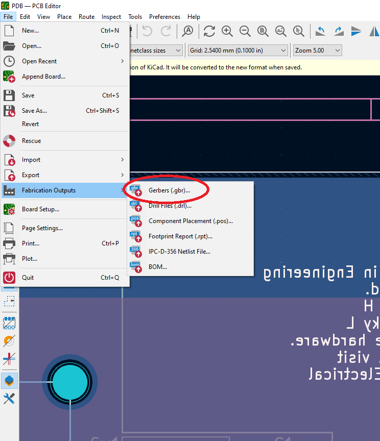
  2. Go to File -> Fabrication Outputs -> Gerbers (.gbr)...
  3. If this is your first time using KiCad, it will prompt you to configure the Global Symbol Library. It is highly recommended that you select "Copy default global symbol library table".
  4. Select the folder icon near the bottom left and navigate to the PiE_Symbols.kicad_sym file in the src folder.
  5. You should now see the PiE_Symbols in your Symbol Libraries. Make sure the "active" box is checked, and click "OK".
  6. Open the brd file

  7. Click Cam Job

  8. Open pie.cam

  9. Make a directory in each sensor's folder called SENSOR_NAME-gerb

    • SENSOR_NAME must be the exact name as the brd file
  10. Run job, and click yes to all for the polygon issue

  11. Once all the jobs are done, run make gerb

Back to Top

FAQ

Q: What's the difference between commit before I pull?

A: Do you want to keep any of the changes? Then commit those (the ones you want to keep) before you pull. Or else, the things you pull might conflict with your work, and you'll have a git disaster.

Q: I worked on my stuff, pulled, and everything I did went away!

A: As long as you committed, the PMs can recover your work for you.

Q: Why am I working on my own branch?

A: This is to keep track of pull request and board reviews on a per board basis

Back to Top

Useful Links

PiE's own Github Tutorial

PiElectrical Wiki

Markdown Cheatsheet

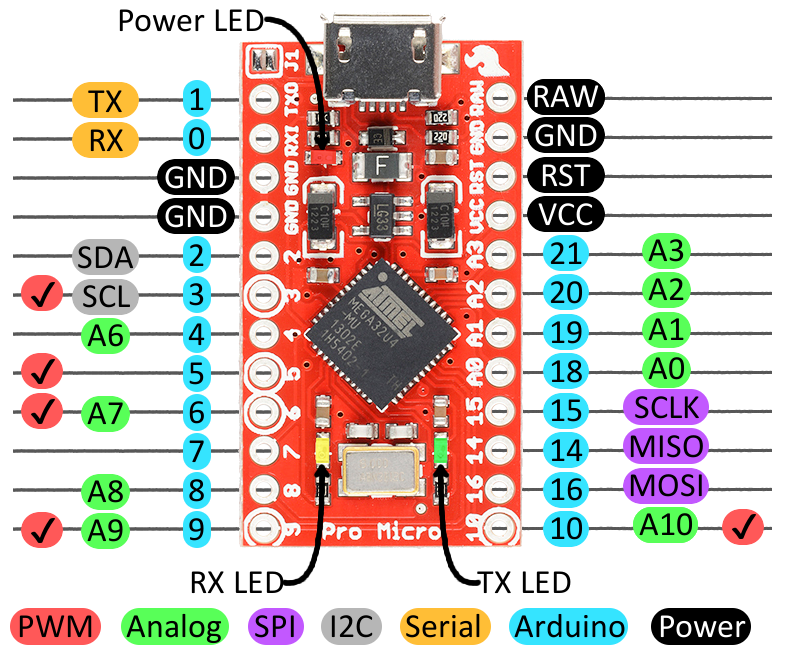
Arduino Pro Micro Pinouts

BAC DFM

Read up on the PiE Electrical Style Rules and Guidelines (This is a good resource, but outdated)

Back to Top

Design Rules

You can find JLC's design rules here: https://jlcpcb.com/capabilities/pcb-capabilities. Please review this before ordering a PCB.

Some of our general rules:
  • Traces must be multiples of 45 degrees
  • Standard Pin Distance: 100 mils (2.54 mm)
Make sure to annotate your boards:
text
Copyright (c) 2023, Pioneers in Engineering
All rights reserved.

Design by: Justin H
This design is open source hardware.
For more information, visit 
github.com/pioneers/PiElectrical

Back to Top

Parts

104
QtyValueFootprintReferences
8200Resistor_SMD:R_0603_1608MetricR7, R8, R9, R10, R11, R12, R13, R14
6330Resistor_SMD:R_0603_1608MetricR26, R27, R28, R29, R30, R31
5100nFCapacitor_SMD:C_0603_1608MetricC8, C9, C10, C11, C16
510kResistor_SMD:R_0402_1005MetricR21, R36, R37, R38, R39
51uFCapacitor_SMD:C_0603_1608MetricC12, C15, C17, C18, C19
5Anderson_HorizontalPiE_Footprints:anderson_horizontalA1, A2, A3, A4, A5
41kResistor_SMD:R_0603_1608MetricR32, R33, R34, R35
4MMBT3906Package_TO_SOT_SMD:SOT-23Q8, Q9, Q10, Q11
4REDLED_SMD:LED_0805_2012MetricD4, D7, D8, D9
4TestPointTestPoint:TestPoint_Loop_D2.60mm_Drill0.9mm_Beaded5V1, GND1, MCU_5V1, USB_VBUS1
310000Resistor_SMD:R_0603_1608MetricR2, R4, R6
3100kResistor_SMD:R_0603_1608MetricR22, R23, R24
32N7002Package_TO_SOT_SMD:SOT-23Q5, Q6, Q7
330000Resistor_SMD:R_0603_1608MetricR1, R3, R5
3BSS84Package_TO_SOT_SMD:SOT-23Q2, Q3, Q4
3USBPiE_Footprints:USB-A_femaleUSB1, USB2, USB3
210uCapacitor_THT:CP_Radial_D5.0mm_P2.00mmC1, C2
218pFCapacitor_SMD:C_0603_1608MetricC13, C14
222Resistor_SMD:R_0603_1608MetricR17, R18
2LM66100DCKPackage_TO_SOT_SMD:SOT-363_SC-70-6U5, U6
11000Resistor_SMD:R_0603_1608MetricR16
110kResistor_SMD:R_0603_1608MetricR25
116MHzCrystal:Crystal_SMD_5032-2Pin_5.0x3.2mmY2
13300Resistor_SMD:R_0603_1608MetricR15
14_digit_7_segment_displayPiE_Footprints:LED-SEG-TH_12P-L30.0-W13.7-P2.54-S10.16-BLD3
15v_converterPiE_Footprints:5v_converterConverter1
1ATmega32U4-MPiE_Footprints:QFN-44-1EP_7x7mm_P0.5mm_EP5.2x5.2mmU4
1AVR-ISP-6Connector_PinHeader_2.54mm:PinHeader_2x03_P2.54mm_VerticalJ4
1BuzzerPiE_Footprints:BuzzerB1
1Conn_01x02PiE_Footprints:PinHeader_1x02_P2.54mm_VerticalJ1
1Conn_01x04PiE_Footprints:PinHeader_1x04_P2.54mm_VerticalJ2
1D-SWITCH_MR5-111-C5N-BBPiE_Footprints:Rocker SwitchSw1
1FuseholderPiE_Footprints:Fuse Holder SMDF1
1GREENLED_SMD:LED_0805_2012MetricD6
1JST-XH_4-pinPiE_Footprints:JST_XH_B4B-XH-A_1x04_P2.50mm_VerticalJst1
1LOGOPiE_Footprints:PiE LogoG***
1RESETButton_Switch_THT:SW_PUSH_6mmSW4
1SW_MEC_5EButton_Switch_THT:SW_PUSH_6mmSW3
1SW_SPDTPiE_Footprints:DEALON SS-12D01-G3SW2
1USBLC6-2SC6Package_TO_SOT_SMD:SOT-23-6U7
1USB_BPiE_Footprints:USB_B_OST_USB-B1HSxx_HorizontalJ3
1XT60_FPiE_Footprints:AMASS_XT60-M_1x02_P7.20mm_VerticalBatt1
1YELLOWLED_SMD:LED_0805_2012MetricD5
1s8050_JSMSEMIPiE_Footprints:s8050 JSMSEMIQ1

The 100 most common of 104 parts.

More from pioneers/PiElectrical

12
  • 2 layers112.1 × 88.3 mmPDB, the printed circuit board in 3D

    PDB

    pioneers/PiElectrical

    PiElectrical Work and Documentation

    77 parts8
  • 2 layers112.1 × 88.3 mmPDB, the printed circuit board in 3D

    PDB

    pioneers/PiElectrical

    PiElectrical Work and Documentation

    59 parts8
  • 2 layers109.5 × 59 mmGabesam board, the printed circuit board in 3D

    Gabesam board

    pioneers/PiElectrical

    PiElectrical Work and Documentation

    25 parts8
  • 2 layers53.3 × 27 mmDC DC converter v2, the printed circuit board in 3D

    DC DC converter v2

    pioneers/PiElectrical

    PiElectrical Work and Documentation

    21 parts8
  • 2 layers104.4 × 58.1 mmSimon Says, the printed circuit board in 3D

    Simon Says

    pioneers/PiElectrical

    PiElectrical Work and Documentation

    18 parts8
  • 2 layersTurbo PCB Design, the printed circuit board in 3D

    Turbo PCB Design

    pioneers/PiElectrical

    PiElectrical Work and Documentation

    15 parts8
  • 2 layers34.9 × 34.7 mmDC DC converter, the printed circuit board in 3D

    DC DC converter

    pioneers/PiElectrical

    PiElectrical Work and Documentation

    14 parts8
  • 2 layers26 × 32 mmUSBTTL, the printed circuit board in 3D

    USBTTL

    pioneers/PiElectrical

    PiElectrical Work and Documentation

    13 parts8
  • 2 layers45.7 × 50.8 mmPiE team flag, the printed circuit board in 3D

    PiE team flag

    pioneers/PiElectrical

    PiElectrical Work and Documentation

    12 parts8
  • 2 layers40.3 × 52.4 mmServocontrollerproject, the printed circuit board in 3D

    Servocontrollerproject

    pioneers/PiElectrical

    PiElectrical Work and Documentation

    10 parts8
  • 2 layers18 × 31 mmUSBTTL, the printed circuit board in 3D

    USBTTL

    pioneers/PiElectrical

    PiElectrical Work and Documentation

    8 parts8
  • 2 layers40.5 × 45.8 mmUltrasonic, the printed circuit board in 3D

    Ultrasonic

    pioneers/PiElectrical

    PiElectrical Work and Documentation

    4 parts8

Similar boards

  • 4 layers120 × 100 mmCryocooler, the printed circuit board in 3D

    Cryocooler

    jhyland87/Cryocooler-Controller

    Control system for STI Hybrid-98 Stirling cycle cryocooler.

    338 parts2
  • 4 layers40.5 × 100 mmVcafd, the printed circuit board in 3D

    Vcafd

    GuavTek/ACID_VCA

    A eurorack VCA with a wavefolder and drive/clipping

    223 parts1CERN-OHL-W-2.0
  • 2 layers43.4 × 63 mmTapper, the printed circuit board in 3D

    Tapper

    rabinniroula/tapper-hw

    KiCad Design Files for Tapper: A hardware tool for LF and HF RFID read, emulation and much more...

    106 parts
  • 2 layers100 × 63.7 mmFcart, the printed circuit board in 3D

    Fcart

    hi0t/fcart

    Open source flash cartridge

    115 parts23GPL-3.0
  • 4 layers112 × 75 mmKvm board, the printed circuit board in 3D

    Kvm board

    FuNK3Y/picoKVM

    A network KVM that can switch inputs of smart monitors

    95 parts6
  • 4 layers35 × 18 mmRingOne, the printed circuit board in 3D

    RingOne

    TheColonelYoung/RingOne

    3D air mouse based on STM32 - Can be used for controlling CADs and every other manipulation in 3D space. Is based around STM32L452, IMU LSM6DSL (gyroscope and accelerometer) and Bluetooth low power module RN4871.

    85 parts3
  • 4 layers48.9 × 49.8 mmFC REV2, the printed circuit board in 3D

    FC REV2

    xXsenseiXx/KHATAF-F411

    Open-hardware 4-layer STM32F411 drone flight controller designed in KiCad for INAV and Betaflight.

    73 parts2
  • 2 layers30 × 30 mmLogger, the printed circuit board in 3D

    Logger

    Birb-jpg/stm32logger

    A 1in.^2 STM32 based flight data logger.

    62 parts

Questions

How big is the PDB PCB?

It measures 112.1 × 88.2 mm and has 2 copper layers, 1.6 mm thick.

What parts does the PDB use?

104 parts, built around the ATMEGA32U4-MU, LM66100DCK, USBLC6-2SC6 and MMBT3906. The full list of its parts is on this page, with links to each part's symbol and footprint where PCBKit's library has them.

Where can I download the PDB KiCad files?

From the pioneers/PiElectrical repository on GitHub, at the commit this page was made from: the board is Boards/PiEDB-Y19/PDB/PDB.kicad_pcb. PCBKit opens the board in the browser, with nothing to install.

Can I use the PDB design in my own project?

Its repository states no licence, so its author keeps all rights: ask pioneers before reusing the design.