Skip to the content
PCBKitNew board
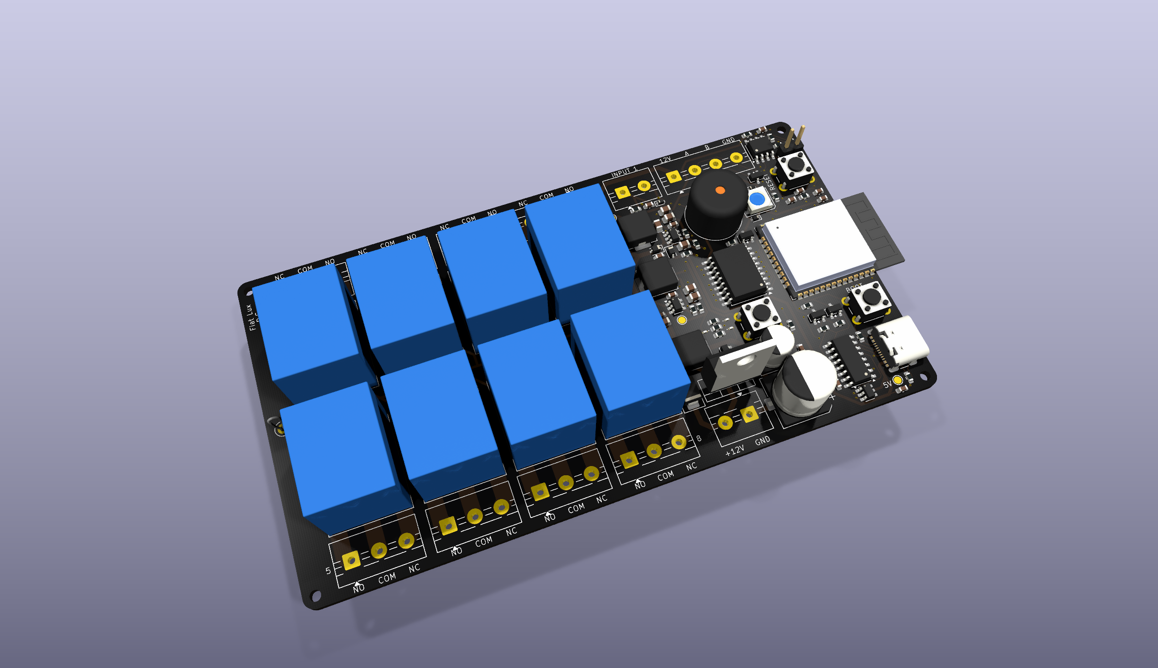
2 layers124.8 × 68 mmESP-32-RELAY CONTROLLER, the printed circuit board in 3D

ESP-32-RELAY CONTROLLER

pasachan/ESP-32-RELAY-CONTROLLER1

An 8-channel relay controller with Wi-Fi, an RS-485 field bus, and a 12 V power rail for downstream nodes. Designed as the master board for a small home-automation network: this board switches loads directly, talks to the outside world over Wi-Fi, and powers and polls a chain of low-cost slave boards (ATtiny / STM32 class) over RS-485.

Size
124.8 × 68 mm
Copper layers
2
Thickness
1.6 mm
Parts
106
Nets
112
Pads
383
Tracks, vias
802, 91
Pours
1
Routed
Yes
KiCad
KiCad 10.0 (file 20260206)
Created
21 Sep 2026
Updated
6 Oct 2026

Overview

ESP-32-RELAY CONTROLLER is an open-source printed circuit board by pasachan, from the pasachan/ESP-32-RELAY-CONTROLLER repository on GitHub, published under the CERN-OHL-P-2.0 licence. It is a 2-layer board of 124.8 × 68 mm with 106 parts on 112 nets, routed with 802 tracks and 91 vias.

It is built around the CH340C, ESP32-WROOM-32D and MAX3485AEASA+T, with the ULN2803A, USBLC6-2SC6 and SRD-S-105D among its other parts. Its parts include 23 capacitors, 23 resistors, 12 diodes, 12 connectors and 11 switches. It belongs with the home automation and IoT boards and the ESP32 boards of this library.

Main components

12

README

README.md

ESP32 Relay Controller

An 8-channel relay controller with Wi-Fi, an RS-485 field bus, and a 12 V power rail for downstream nodes. Designed as the master board for a small home-automation network: this board switches loads directly, talks to the outside world over Wi-Fi, and powers and polls a chain of low-cost slave boards (ATtiny / STM32 class) over RS-485.

Board render

Open hardware. KiCad 10 source, fabrication outputs, BOMs with LCSC part numbers, and a pick-and-place file are all in this repository. Rev 1 has been manufactured.


Features

  • ESP32-WROOM-32D (16 MB flash) — Wi-Fi + Bluetooth, USB-C programming via CH340C with auto-reset
  • 8 × SPDT relays (SRD-05VDC, 10 A contacts), driven by a ULN2803A with built-in flyback clamps, each brought out to a 3-way screw terminal (NO / COM / NC)
  • RS-485 half-duplex master — MAX3485 (3.3 V), SM712 surge protection, jumper-selectable 120 Ω termination, fail-safe biasing
  • 12 V field bus power on the RS-485 connector, so slave nodes need no local supply
  • 12 V input with P-FET reverse-polarity protection, bidirectional TVS, and an LC input filter
  • Two synchronous bucks (LMR51430): 5 V for relay coils, 3.3 V for logic — the 3.3 V rail also runs from USB alone for bench programming
  • One dry-contact input (pull-up, RC filter, ESD clamp), active buzzer, WS2812B status LED, rail indicator LEDs
  • RESET / BOOT / user (WPS) buttons, 2 mm mounting holes, 124.75 × 68 mm, 2-layer

Block diagram

mermaid
flowchart LR
    J1["12 V input"] --> Q1["IRF4905<br/>reverse-polarity FET"] --> L3["LC input filter"] --> V12["+12 V rail"]
    D2["SMBJ18CA TVS"] -.clamps.-> J1
    V12 --> U2["LMR51430<br/>buck → 5 V"] --> V5["+5 V coil rail"]
    V12 --> D3["Schottky OR"] --> U3["LMR51430<br/>buck → 3.3 V"] --> V33["+3.3 V logic"]
    USB["USB-C"] --> U4["USBLC6 ESD"] --> U6["CH340C"] <-->|"UART0 + auto-reset"| U1
    USB -->|"VBUS"| D4["Schottky OR"] --> U3
    V33 --> U1["ESP32-WROOM-32D"]
    U1 -->|"8 × GPIO"| U7["ULN2803A"] -->|"8 × coil"| K["K2 … K9<br/>SRD-05VDC SPDT"] --> JT["8 × NO/COM/NC<br/>screw terminals"]
    V5 --> K
    U1 <-->|"UART2 + DE/RE"| U9["MAX3485<br/>RS-485"] --> D6["SM712 TVS"] --> J12["Field bus<br/>12V · A · B · GND"]
    V12 --> J12
    U1 --> BZ["Buzzer"]
    U1 --> LED["WS2812B"]
    IN["Dry-contact input"] --> U1

Specifications

Supply12 V DC nominal (LMR51430 bucks accept 4–36 V; TVS clamps at 18 V standoff)
Board draw @ 12 V~170 mA idle · ~520 mA worst case (all relays + Wi-Fi TX)
Field-bus power budget~1.8 A at 12 V on J12 — set by the 1.0 mm feed trace (2.4 A @ 10 °C rise) less the board's own draw; L3 is rated 4.5 A
Relay contactsSPDT, 10 A / 250 VAC rated · PCB traces sized for ≤ 2.3 A at 12–30 V (see design notes)
Relay coil drive~4.0 V at the coil vs 3.75 V pick-up spec — all eight channels
RS-485Half-duplex, 3.3 V transceiver, 120 Ω termination via JP1, 330 Ω fail-safe bias (this node only)
USBUSB 2.0 Full Speed (CH340C), USB-C receptacle, 5.1 k CC pull-downs, VBUS ESD array
Logic level3.3 V throughout; WS2812B fed through a series diode so 3.3 V data meets its VIH
Dimensions124.75 × 68 mm, 1.6 mm FR-4, 2 layers, 1 oz copper
Mounting4 × Ø2.0 mm holes at the corners

Repository layout

text
esp32-relay-controller/
├── README.md
├── hardware/
│   ├── kicad/                     KiCad 10 project (schematic, PCB, custom rules, project symbol lib)
│   ├── fabrication/
│   │   ├── gerbers/               RS-274X gerbers + Excellon drill files (fab layers only)
│   │   ├── esp32-relay-controller-gerbers.zip
│   │   ├── BOM.csv                Master BOM — every fitted part, SMD and through-hole, with LCSC + MPN
│   │   ├── BOM-JLCPCB.csv         SMD-only, JLCPCB column format
│   │   ├── BOM-PCBWay.csv         SMD-only, MPN-first for PCBWay
│   │   ├── CPL.csv                SMD pick-and-place (Designator / Mid X / Mid Y / Layer / Rotation)
│   │   └── README.md              How to order
│   └── images/                    Renders and layer plots
├── docs/
│   ├── schematic.pdf
│   ├── design-notes.md            Design decisions, the review process, and what changed as a result
│   └── pinout.md                  ESP32 GPIO map, relay ↔ terminal ↔ GPIO table, connector pinouts
└── firmware/
    ├── README.md                  Pin definitions and the gotchas that bite firmware authors
    └── self-test/                 Bring-up sketch — exercises every component, no libraries needed

Getting boards made

Everything a fab needs is in hardware/fabrication/. The short version:

  1. Upload esp32-relay-controller-gerbers.zip for the bare PCB — 2 layer, 1.6 mm, 1 oz, any colour.
  2. For SMD assembly, upload BOM-JLCPCB.csv + CPL.csv (JLCPCB) or BOM-PCBWay.csv + CPL.csv (PCBWay). 72 SMD parts, 35 lines.
  3. Hand-fit the 25 through-hole parts: 8 relays, 11 screw-terminal blocks, the TO-220 FET, buzzer, three tact switches and the termination header. All are common parts; LCSC numbers are in BOM.csv.

See hardware/fabrication/README.md for gerber-origin caveats, the one DFM query a fab may raise, and which parts are safe to substitute.


Firmware quick reference

firmware/self-test/ is a bring-up sketch that exercises every fitted component and prints a pass/fail report over USB serial. Run it first on a new board. Full map in docs/pinout.md, gotchas in firmware/README.md.

FunctionGPIONotes
Relay 1 … 8 (silkscreen order)14, 19, 25, 13, 23, 33, 32, 18Active-high into ULN2803A
RS-485 TX / RX / DE+RE17 / 16 / 2GPIO2 has a 10 k pull-down → receive mode at boot
Dry-contact input34Input-only pin, external 10 k pull-up, closes to GND
User button (WPS)35Input-only, 10 k pull-down, pressed = high
Buzzer26Via NPN, active-high
WS2812B data27Through 330 Ω
UART0 (USB)1 / 3CH340C with DTR/RTS auto-reset
I²C21 / 22Routed to pads but no pull-ups fitted in rev 1

Design notes

The interesting engineering is in docs/design-notes.md. Highlights:

  • Why the field bus carries 12 V and not 3.3 V — cable drop and the thermal ceiling of a SOT-23-6 buck make 3.3 V distribution a dead end past a couple of nodes; regulating at each slave costs one LDO and removes the constraint.
  • Reverse-polarity protection with a P-FET, and why the TVS sits in front of it — a unidirectional clamp ahead of the FET would short a reversed supply, so it's a bidirectional part.
  • Relay coil drive margin — the SRD-05VDC needs 3.75 V to pull in; behind a ULN2803A the coil sees ~4.0 V. A series diode in the original design put one channel under the limit and was removed.
  • Driving a 5 V WS2812B from a 3.3 V GPIO — a diode in the LED's supply drops VDD into the window where 3.3 V is a valid high, without a level shifter.
  • A KiCad DRC gotcha — custom rules that match on auto-generated net names like Net-(J2-Pin_1) silently never fire. The rules in this project match on a netclass instead.
  • What the design review caught — the board went through a full netlist, DRC, ERC and geometric-connectivity audit before ordering; the findings and fixes are documented.

Status

RevisionDateNotes
Rev 1Sep 2026Ordered. 0 DRC errors, 0 unconnected nets, all nets verified single-island.
Rev 1Oct 2026Built and brought up. All eight relays, the buzzer, the WS2812B, both inputs, the RS-485 receiver and the USB programming path work. One firmware-level finding: the MAX3485's RO pin is tri-stated during transmit and has no pull-up, so it needs one enabled in software — details.

Known rev 1 limitations and the planned rev 2 changes are listed at the end of the design notes.


Licence

Copyright © 2026 Pareekshit Sachan.

This source describes Open Hardware and is licensed under the CERN-OHL-P v2 (SPDX-License-Identifier: CERN-OHL-P-2.0). You may redistribute and modify this documentation and make products using it under the terms of the CERN-OHL-P v2 — see LICENSE or https://cern.ch/cern-ohl.

This documentation is distributed WITHOUT ANY EXPRESS OR IMPLIED WARRANTY, INCLUDING OF MERCHANTABILITY, SATISFACTORY QUALITY AND FITNESS FOR A PARTICULAR PURPOSE. Please see the CERN-OHL-P v2 for applicable conditions.

Symbols, footprints and 3D models from the KiCad libraries are used under the KiCad library licence (CC-BY-SA 4.0 with exception). Datasheets referenced in the design notes remain the property of their manufacturers.

Parts

106
QtyValueFootprintReferences
10100nf 50VCapacitor_SMD:C_0603_1608MetricC3, C4, C5, C6, C9, C14, C17, C18, C23, C25
8SRD-S-105DRelay_THT:Relay_SPDT_SANYOU_SRD_Series_Form_CK2, K3, K4, K5, K6, K7, K8, K9
8Screw_Terminal_01x03TerminalBlock:TerminalBlock_MaiXu_MX126-5.0-03P_1x03_P5.00mmJ2, J3, J4, J6, J8, J9, J10, J11
410KResistor_SMD:R_0603_1608MetricR8, R9, R24, R25
422uf 16vCapacitor_SMD:C_0805_2012MetricC7, C8, C10, C11
4330Resistor_SMD:R_0603_1608MetricR26, R27, R37, R42
4MountingHoleMountingHole:MountingHole_2mmH1, H2, H3, H4
3100kResistor_SMD:R_0603_1608MetricR1, R3, R5
310kResistor_SMD:R_0603_1608MetricR10, R15, R22
310uf 50VCapacitor_SMD:C_0805_2012MetricC12, C13, C15
34.7kResistor_SMD:R_0603_1608MetricR14, R18, R40
3SS8050Package_TO_SOT_SMD:SOT-23Q2, Q3, Q5
210uF 25VCapacitor_SMD:C_0603_1608MetricC21, C22
21N4148WT-7Diode_SMD:D_SOD-523D1, D13
21uF 50VCapacitor_SMD:C_0603_1608MetricC19, C20
25.1kResistor_SMD:R_0603_1608MetricR6, R7
2BOOT LEDLED_SMD:LED_0201_0603MetricD7, D11
2CUS10S30Diode_SMD:D_SOD-323D3, D4
2LMR51430Package_TO_SOT_SMD:SOT-23-6U2, U3
1100uf 35vCapacitor_SMD:CP_Elec_6.3x7.7C2
110uH 4.5AInductor_SMD:L_Changjiang_FXL0630L3
112 V ProtectedTestPoint:TestPoint_Pad_D1.5mmTP1
1120Resistor_SMD:R_0603_1608MetricR23
113.7kResistor_SMD:R_0603_1608MetricR2
11kResistor_SMD:R_0603_1608MetricR38
122.1kResistor_SMD:R_0603_1608MetricR4
13.3VTestPoint:TestPoint_Pad_D1.5mmTP3
1470uf 35vCapacitor_SMD:CP_Elec_10x10.5C1
15.6uhInductor_SMD:L_Changjiang_FXL0630L2
15VTestPoint:TestPoint_Pad_D1.5mmTP2
15V LEDLED_SMD:LED_0201_0603MetricD9
16.8 uhInductor_SMD:L_Changjiang_FXL0630L1
1BOOTButton_Switch_THT:SW_PUSH_6mmSW2
1BZX84-C16Package_TO_SOT_SMD:SOT-23D5
1CDSOT23-SM712Package_TO_SOT_SMD:SOT-23D6
1CH340CPackage_SO:SOIC-16_3.9x9.9mm_P1.27mmU6
1ESP32-WROOM-32DRF_Module:ESP32-WROOM-32DU1
1GNDTestPoint:TestPoint_Loop_D2.50mm_Drill1.0mmTP4
1IRF4905Package_TO_SOT_THT:TO-220-3_VerticalQ1
1Jumper_2_OpenConnector_PinHeader_2.54mm:PinHeader_1x02_P2.54mm_VerticalJP1
1MAX3485AEASA+TPackage_SO:SOIC-8_3.9x4.9mm_P1.27mmU9
1PESD3V3S1UBDiode_SMD:D_SOD-523D8
1Power Input +12VTerminalBlock:TerminalBlock_MaiXu_MX126-5.0-02P_1x02_P5.00mmJ1
1RESETButton_Switch_THT:SW_PUSH_6mmSW1
1S1TerminalBlock:TerminalBlock_MaiXu_MX126-5.0-02P_1x02_P5.00mmJ7
1SMBJ18CADiode_SMD:D_SMBD2
1Screw_Terminal_01x04TerminalBlock:TerminalBlock_MaiXu_MX126-5.0-04P_1x04_P5.00mmJ12
1TMB12A05Buzzer_Beeper:Buzzer_12x9.5RM7.6Buzzer1
1ULN2803APackage_SO:SOIC-18W_7.5x11.6mm_P1.27mmU7
1USBLC6-2SC6Package_TO_SOT_SMD:SOT-23-6U4
1USB_5VTestPoint:TestPoint_Pad_D1.5mmTP10
1USB_C_Receptacle_USB2.0_16PConnector_USB:USB_C_Receptacle_GCT_USB4105-xx-A_16P_TopMnt_HorizontalJ5
1WPSButton_Switch_THT:SW_PUSH_6mmSW3
1WS2812BLED_SMD:LED_WS2812B_PLCC4_5.0x5.0mm_P3.2mmD15

Questions

How big is the ESP-32-RELAY CONTROLLER PCB?

It measures 124.8 × 68 mm and has 2 copper layers, 1.6 mm thick.

What parts does the ESP-32-RELAY CONTROLLER use?

106 parts, built around the CH340C, ESP32-WROOM-32D, MAX3485AEASA+T and ULN2803A. The full list of its parts is on this page, with links to each part's symbol and footprint where PCBKit's library has them.

Where can I download the ESP-32-RELAY CONTROLLER KiCad files?

From the pasachan/ESP-32-RELAY-CONTROLLER repository on GitHub, at the commit this page was made from: the board is hardware/kicad/esp32-relay-controller.kicad_pcb and its schematic hardware/kicad/esp32-relay-controller.kicad_sch. PCBKit opens the board in the browser, with nothing to install.

Can I use the ESP-32-RELAY CONTROLLER design in my own project?

Its repository publishes it under the CERN-OHL-P-2.0 licence: you may reuse it on that licence's terms (keep the author's notice, and for a copyleft licence share your changes alike).

Similar boards

  • 2 layers60.5 × 95 mmPhylax Version 3, the printed circuit board in 3D

    Phylax Version 3

    ta007403/PHYLAX

    PHYLAX (Greek φύλαξ, "guardian") is an open-source, Bitcoin-only hardware wallet built around a simple idea: no black-box chips, no wireless radios, no telemetry, and firmware you can read and verify yourself.

    65 parts
  • 4 layers123.8 × 76.2 mmBalloonMotherboardV3, the printed circuit board in 3D

    BalloonMotherboardV3

    EggiEl/SpiCy-BEXUS

    Cyanobacteria are among the oldest and most efficient photosynthetic organisms on planet Earth. They contribute 25% of the oxygen on Earth today and were crucial in forming our atmosphere in the early stages of Earth's…

    198 parts1
  • 4 layers100 × 150 mmBeepyRcBrd only top, the printed circuit board in 3D

    BeepyRcBrd only top

    ElectronPlant/beepy_rc

    Hobby project to make a RC rover platform using spare RC parts.

    173 parts
  • 12 layers160.1 × 233.5 mmVme wren, the printed circuit board in 3D

    Vme wren

    KiCad/kicad-source-mirror

    This is an active mirror of the KiCad development branch, which is hosted at GitLab (updated every time something is pushed). Pull requests on GitHub are not accepted or watched.

    1,508 parts3.1kGPL-3.0
  • 4 layers135.8 × 149.3 mmTapBadgeV2, the printed circuit board in 3D

    TapBadgeV2

    Xasin/TapBadgeV2

    The second, far more ambitious version of the TapBadge wearable

    110 parts6GPL-3.0
  • 2 layers80 × 30 mmController PCB, the printed circuit board in 3D

    Controller PCB

    h2dakhil/FFT-Audio-Spectrum-Analyzer

    Real-time audio-reactive LED matrix powered by an ESP32, featuring custom PCB design, I2S microphone input, and dynamic visual effects through FFT signal processing.

    42 parts
  • 2 layers200 × 170 mmRav4-tcu, the printed circuit board in 3D

    Rav4-tcu

    gamer927/rav4

    rav4

    118 parts
  • 2 layers118 × 70 mmPhotogateV2, the printed circuit board in 3D

    PhotogateV2

    MarcioBulla/PhotogateV2

    Second Version of Photogate

    66 parts1