
2 layers99.8 × 55.9 mm

 Parahybaja/hardware
The Accelaration and Velocity test module
Module is an open-source printed circuit board by Parahybaja, from the Parahybaja/hardware repository on GitHub, published under the MIT licence. It is a 2-layer board of 66 × 71.8 mm with 23 parts on 41 nets, routed with 71 tracks and 331 vias.
It is built around the ESP32-DEVKITC-VE. Its parts include 7 capacitors, 4 resistors, 4 connectors, 2 diodes and 2 inductors. It belongs with the ESP32 boards of this library.
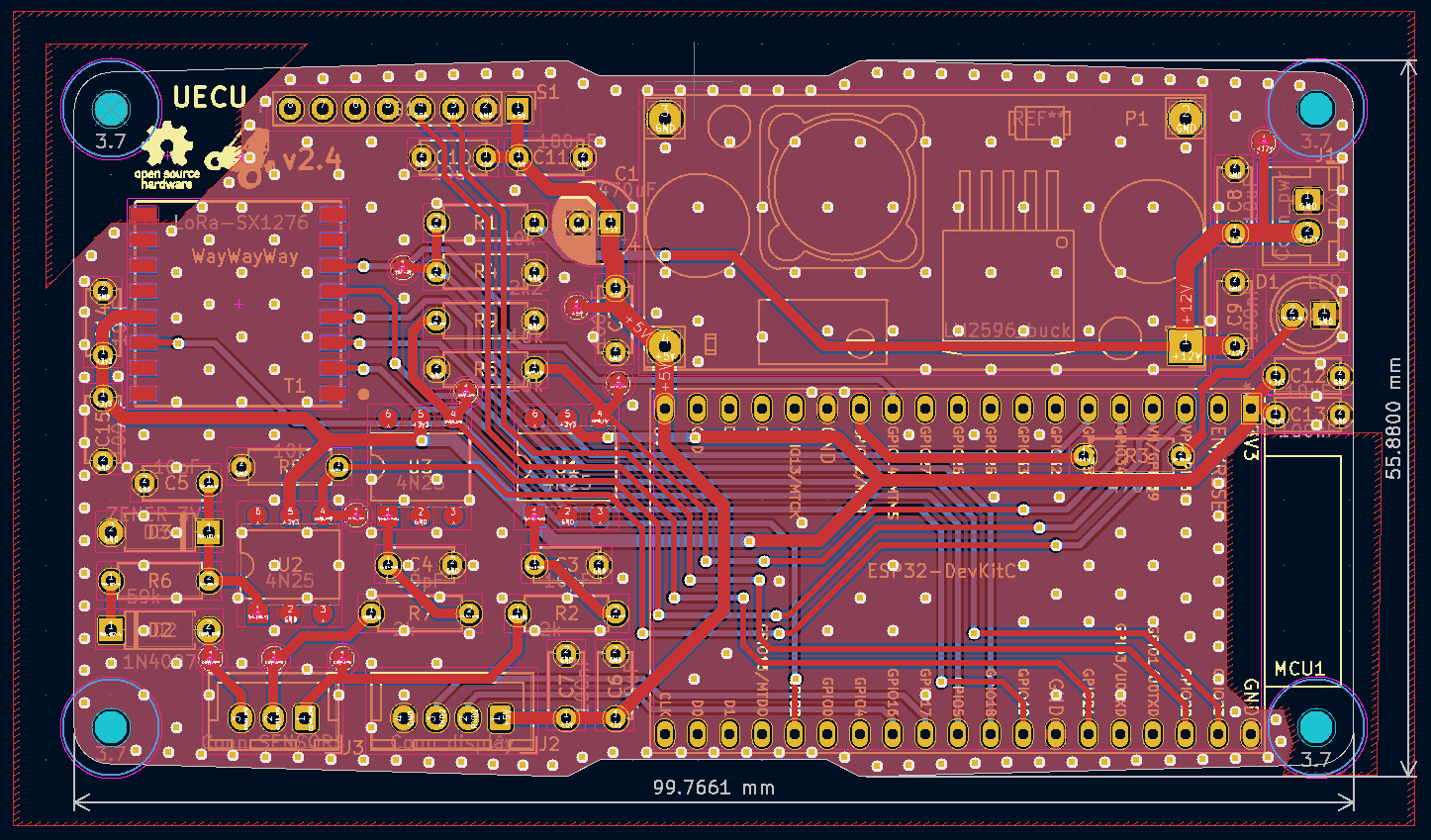
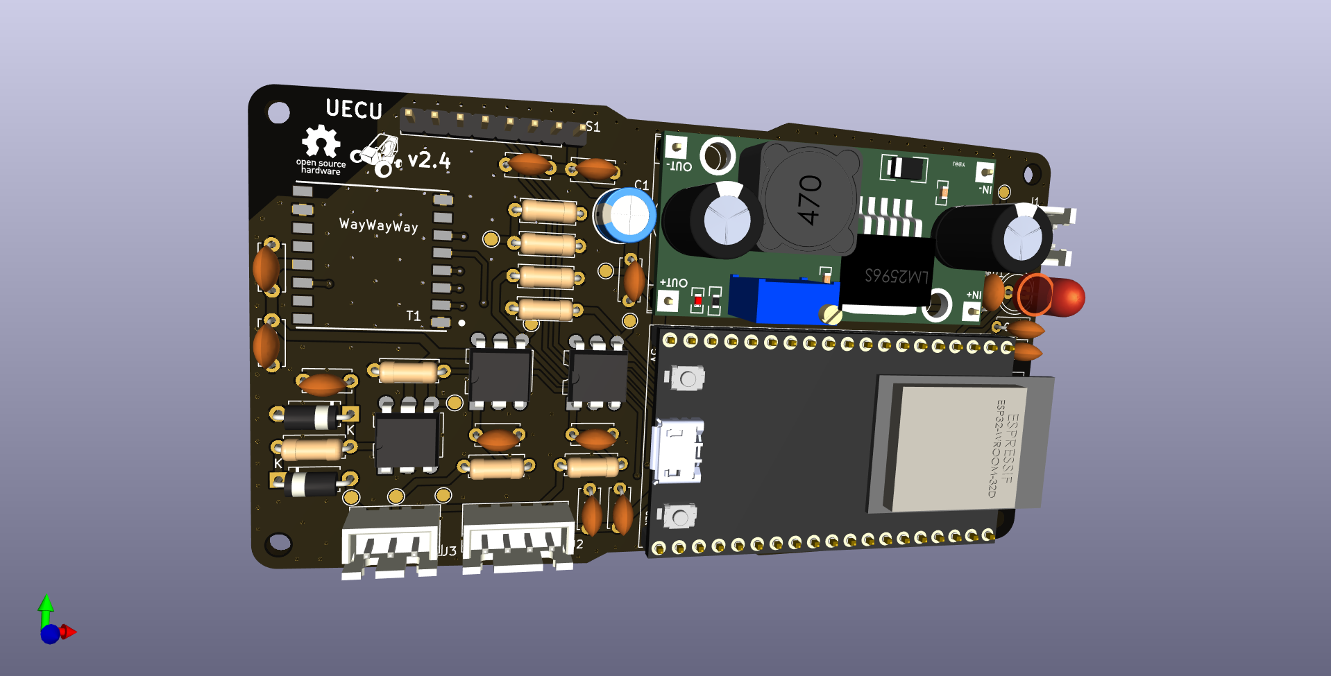
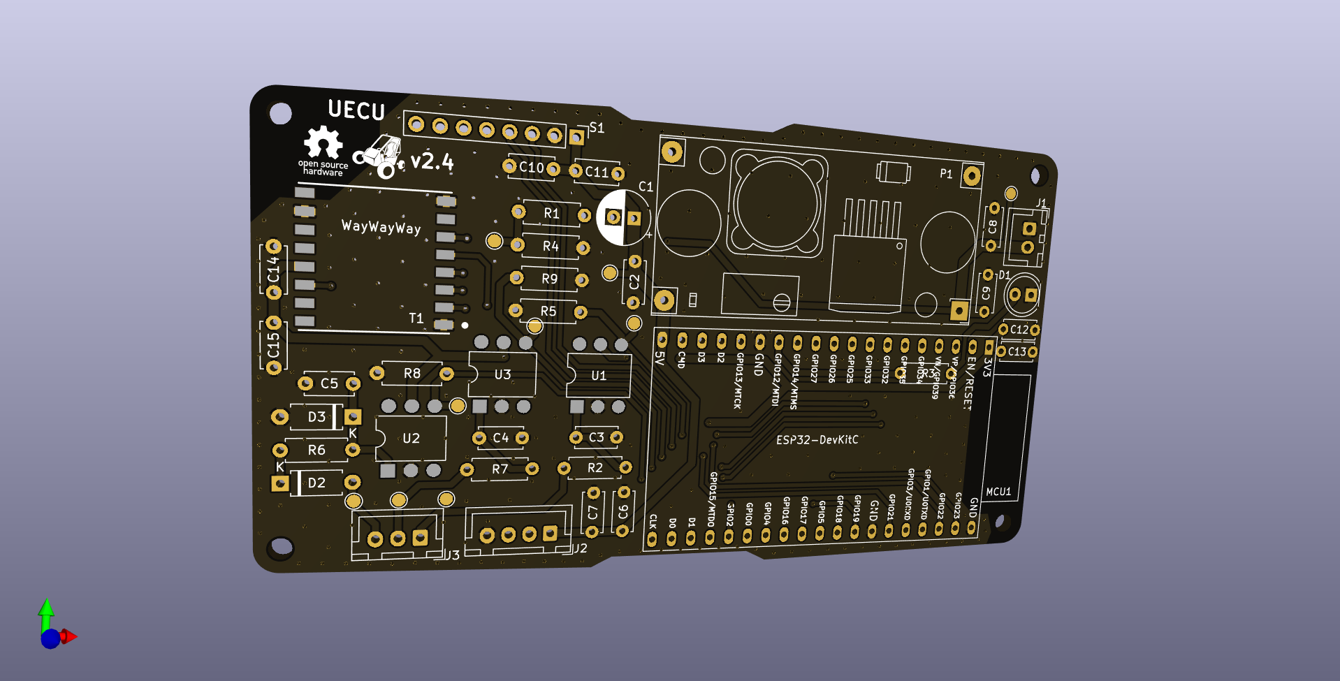
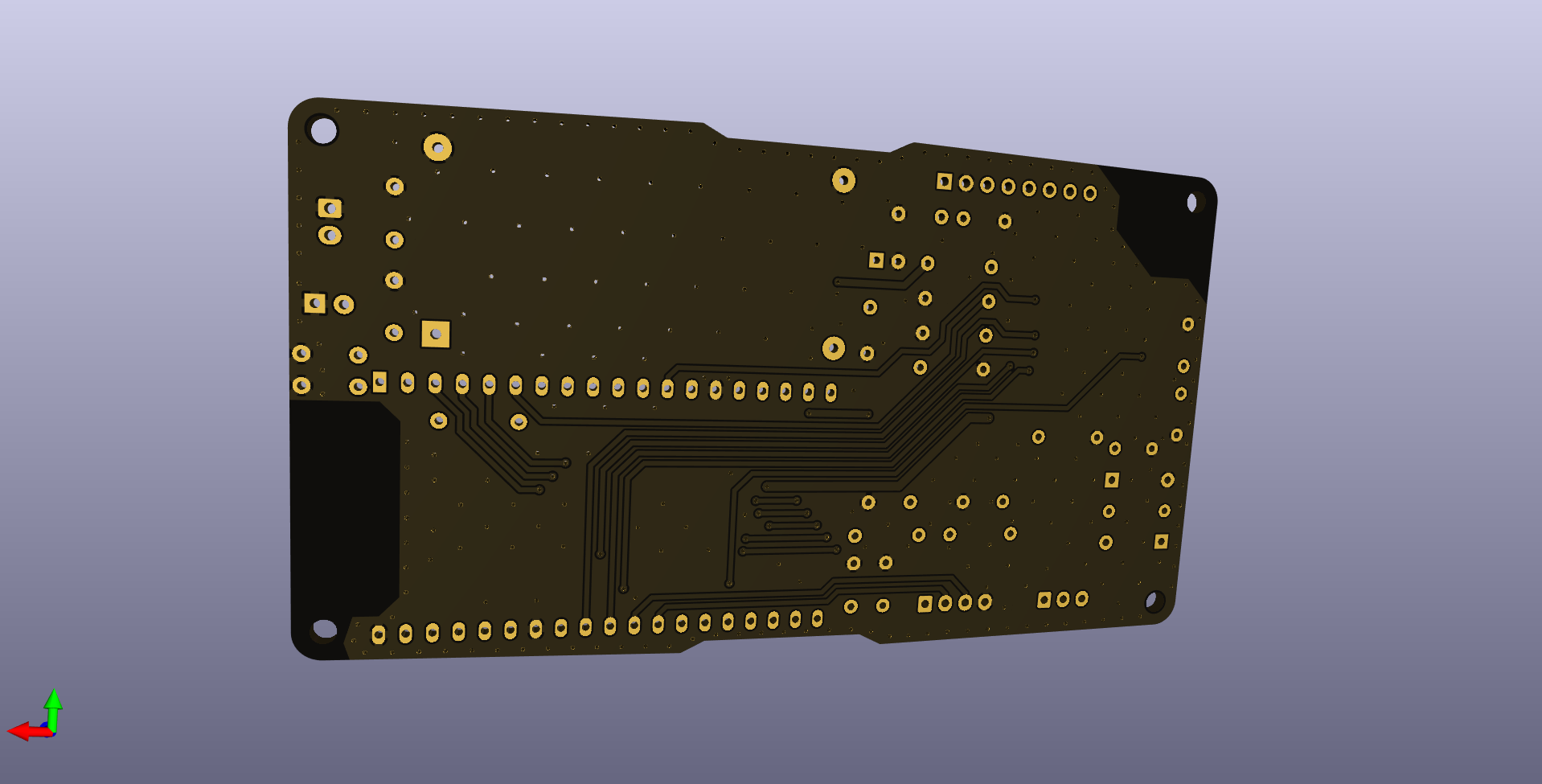
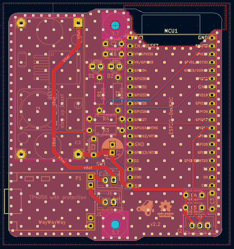
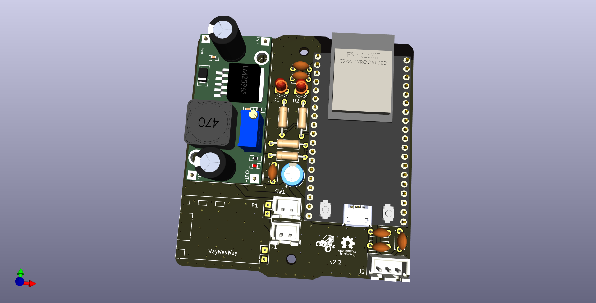
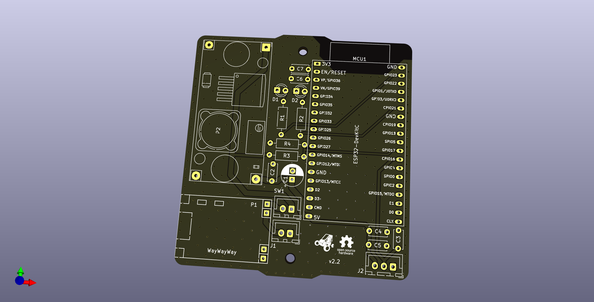
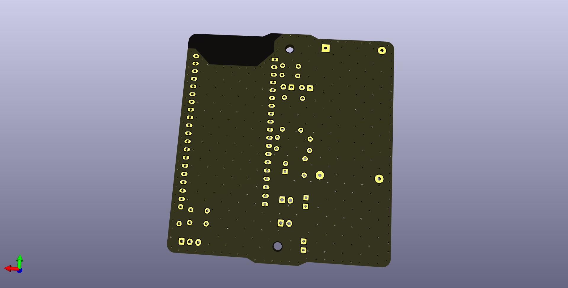
Universal Electronics Control Unit
The Accelaration and Velocity test module
A signal cleaning stage was employed in the digital inputs of each sensor with the aim of eliminating electromagnetic interference in the data transmission line. For this purpose, a passive low-pass filter with a cutoff frequency of 1GHz was implemented.
To achieve the desired cutoff frequency, based on a resistor of 2.2k ohms, chosen to maintain the optimal current for the optocoupler's LED, the following calculations were made:
$$ F_c = \frac{1}{{2 \pi R C}} $$
$$ C = \frac{1}{{F_c \cdot 2 \pi R}} $$
$$ C = \frac{1}{{1 \text{GHz} \cdot 2 \pi \cdot 2.2k}} $$
$$ C \approx 72 \text{pF} $$
| Qty | Value | Footprint | References |
|---|---|---|---|
| 3 | 100nF | Capacitor_THT:C_Disc_D5.0mm_W2.5mm_P5.00mm | C2, C5, C7 |
| 2 | 10uF | Capacitor_THT:C_Disc_D5.0mm_W2.5mm_P5.00mm | C4, C6 |
| 2 | 3.7 | MountingHole:MountingHole_3.7mm | H1, H2 |
| 2 | 300R | Resistor_THT:R_Axial_DIN0207_L6.3mm_D2.5mm_P10.16mm_Horizontal | R1, R2 |
| 2 | R_Small | Resistor_THT:R_Axial_DIN0207_L6.3mm_D2.5mm_P10.16mm_Horizontal | R3, R4 |
| 1 | 22pF | Capacitor_THT:C_Disc_D5.0mm_W2.5mm_P5.00mm | C3 |
| 1 | 470uF | Capacitor_THT:CP_Radial_D6.3mm_P2.50mm | C1 |
| 1 | Conn_bat | Connector_JST:JST_XH_B3B-XH-A_1x03_P2.50mm_Vertical | J2 |
| 1 | Conn_bat | Connector_JST:JST_XH_B2B-XH-A_1x02_P2.50mm_Vertical | J1 |
| 1 | Conn_sw | Connector_JST:JST_XH_B2B-XH-A_1x02_P2.50mm_Vertical | SW1 |
| 1 | ESP32-DevKitC | Espressif:ESP32-DevKitC | MCU1 |
| 1 | LEDG | LED_THT:LED_D3.0mm | D2 |
| 1 | LEDR | LED_THT:LED_D3.0mm | D1 |
| 1 | TP4056 with protection | Battery_charger:TP4056 | P1 |
| 1 | step up boost | StepDown:StepDown_LM2596 | P2 |
| 1 | ~ | Logos:parahybaja | L1 |
| 1 | ~ | Logos:open_hardware | L2 |

harbaum/galagino
A Galaga, Pac-Man and Donkey Kong arcade emulator for the ESP32

RParkerE/OpenSilicon
OpenSilicon enables DIY semiconductor fabrication with open-source guides for building IC equipment at home. The project includes BOMs, 3D files, firmware, and PDKs, supporting makers and researchers in chip fabrication.

cole8888/SRNE-Solar-Charge-Controller-Monitor
Read data from SRNE solar charge controllers.


ste2425/PSP-Bluetooth-AVConnector
An AV-Out Breakout library for the PSP. Providing Kicad symbols and footprints to interface with the PSP 2/3K AVOut socket (also known as the TVOut socket)

It measures 66 × 71.8 mm and has 2 copper layers, 1.6 mm thick.
23 parts, built around the ESP32-DEVKITC-VE. The full list of its parts is on this page, with links to each part's symbol and footprint where PCBKit's library has them.
From the Parahybaja/hardware repository on GitHub, at the commit this page was made from: the board is module/module.kicad_pcb and its schematic UECU/UECU.kicad_sch. PCBKit opens the board in the browser, with nothing to install.
Its repository publishes it under the MIT licence: you may reuse it on that licence's terms (keep the author's notice, and for a copyleft licence share your changes alike).