

2 layers309.9 × 119.8 mm
Cockpit
ozkan/Cockpit-Keyboard
A hot swap system column staggered mechanical keyboard, running QMK Firmware on Pro Micro controllers.
144 parts43MIT

 Pacane/pacino3
Hand-wired wireless split keyboard: printable OpenSCAD case/plate with STEP output for Fusion 360. Cheapino-descended layout, nRF52840 + ZMK, Amoeba-King hot-swap.
Pacino flat is an open-source printed circuit board by Pacane, from the Pacane/pacino repository on GitHub, published under the MIT licence. It is a 2-layer board of 139.1 × 114.3 mm with 49 parts on 39 nets, routed with 557 tracks and 21 vias.
It is built around the 1N4148W and SS-12D00-G3. Its parts include 20 diodes, 20 switches and 1 IC. It belongs with the keyboards and input boards and the nRF52 and nRF5x boards of this library.
The board for the slim build whose cell sits in a well in the case floor, entirely under the board -- the plate is flat.
Cell: 303040 (3 x 30 x 40, ~320 mAh). Case half: variants/5col_extra2_bat303040_pcb_flat.
The two slim builds are two boards, not one board with an option: moving the cell moves the bay, two of the mounting holes and the reset/power positions. The matrix, the footprints and the firmware are identical between them.
Generated by tools/pcb_gen.py -- do not hand-edit
pacino_flat.kicad_pcb; change the generator (or keyboard.scad, which the outline and every
position come from) and re-run it. There is no schematic file: the generator declares every net and
every connection, and names the nets the way the ZMK shield names them.
tools/pcb_gen.py                 # both boards, with gerbers and renders
tools/pcb_gen.py --variant=flat  # just this one
tools/pcb_gen.py --no-render     # skip the raytracing while iterating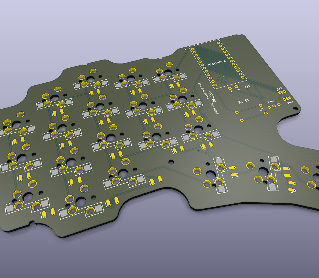
20 keys, 39 nets, 557 tracks, 21 vias. Two layers, 1.6 mm, 0.3 mm tracks, 0.2 mm clearance, 0.3 mm smallest drill -- inside every fab's cheapest process.
The board is reversible: build the left half with the parts on the back, flip the board over and build the right half with the parts on the front. The silkscreen on each face says which half it is. Three things make that work.
Switches. Every switch footprint carries both MX pin diagonals -- the normal pair and its 180 degree rotation -- and a hot-swap socket land on each face. On the right half the switches and the sockets go in rotated 180 degrees; MX switches are square and their stems are symmetric, so nothing about the feel, the keycaps or the plate changes. (Mirroring the pin pair instead, which is the obvious way to do it, puts two 3 mm holes 2.84 mm apart -- they would merge into a slot.)
Matrix. The controller sits on the face opposite the sockets and diodes -- on top of the board,
component side towards it, flush in the plate's window -- and flipping the board swaps its two pin
rows but not the position along a row, so each hole is one pin on the left half and a different one
on the right. The ten matrix holes were
chosen so that both of their pins are usable GPIOs and neither is one of pro_micro 1/14/15/16 --
the nice!view's CS/MISO/SCK/MOSI stay free on both halves. The two halves therefore need different
pin lists in ZMK -- which is why the slim build has its own shield, pacino_pcb, whose two overlays
differ from each other (the hand-wired pacino shield is unchanged and unrelated):
| net | hole | left half | right half |
|---|---|---|---|
ROW0 | U1 pad 20 | pro_micro 2 | pro_micro 21 |
ROW1 | U1 pad 19 | pro_micro 3 | pro_micro 20 |
ROW2 | U1 pad 18 | pro_micro 4 | pro_micro 19 |
ROW3 | U1 pad 17 | pro_micro 5 | pro_micro 18 |
ROW4 | U1 pad 13 | pro_micro 9 | pro_micro 10 |
COL0 | U1 pad 5 | pro_micro 21 | pro_micro 2 |
COL1 | U1 pad 6 | pro_micro 20 | pro_micro 3 |
COL2 | U1 pad 7 | pro_micro 19 | pro_micro 4 |
COL3 | U1 pad 8 | pro_micro 18 | pro_micro 5 |
COL4 | U1 pad 12 | pro_micro 10 | pro_micro 9 |
Power. RAW and GND have no symmetric partner, so each gets a three-pad solder jumper: bridge the
centre pad to the pad marked L or R for the half you are building. The mark is printed on
the face the controller sits on (the face opposite the sockets), and that is the pad to bridge.
Boards generated before September 2026 have the letters the other way round: on those, still bridge
the marked pad on the controller's face, whatever letter it shows. Reset needs no jumper -- the
switch sits across the (rowA,3)/(rowB,3) pair, which is GND/RST one way up and RST/GND the
other; a 12 mm tactile links its two legs 12.5 mm apart internally, and the footprint puts those on
one net (boards from before the same date have it the other way and short RST to GND: fit the
switch by two diagonal legs only).
| jumper | bridge to | left half | right half |
|---|---|---|---|
JP1 RAW | centre -> L or R | pad 1 = RAW | pad 24 = RAW |
JP2 GND | centre -> L or R | pad 21 = GND | pad 4 = GND |
JP1 and JP2 to the pad marked for your half.BAT + / -; the cell lies in the floor well beneath them.| qty | part | notes |
|---|---|---|
| 20 | Kailh MX hot-swap socket | CPG151101S11, one per key, on the face you assemble |
| 20 | 1N4148W diode | SOD-123; a through-hole 1N4148 on 3.3 mm pitch fits the same land |
| 20 | MX switch | plate-mount 3-pin or PCB-mount 5-pin, 3x 1.25u for the thumbs |
| 1 | nice!nano v2 / nRF52840 SuperMini | component side DOWN on 3.5 mm low-profile sockets |
| 2 | 1x12 machined low-profile socket | Mill-Max and similar; a normal stamped 2.54 header stands ~8.5 mm and will not fit under the plate |
| 2 | 1x12 machined pin strip | into the controller's castellations, pins out of its COMPONENT side. Measure board surface to controller underside with a pin seated: that is mcu_socket_h (3.5 mm by default, and it cannot go below 3.5 -- the USB shell hangs 3.2 mm under the board) |
| 1 | 12x12 mm THT tactile switch | reset, tall plunger, through the plate window |
| 1 | SS12D00 slide switch | power, through the plate window |
| 1 | LiPo cell 303040 (3 x 30 x 40, ~320 mAh) | in a well in the case floor, entirely under the board -- the plate is flat |
Plus, from the case: 8 x M2x3x3.5 heat-set inserts, 8 x M2x10 screws, 8 x 10 mm bumpons.
Five of the eight are half-circles in the edge rather than holes through the board; the other three (the thumb end, the bay's bottom corner and the one between the columns) are real holes. That follows from the case: five of its screw bosses sit 0.5 mm inside the inner wall line so they merge into the wall, and the board is the cavity less 0.5 mm -- so those screws' centres land exactly on the board's edge. The other three bosses stand 2.5-3 mm clear of the wall, because the wall keeps rising past the bosses in this build and an insert hole at the wall line would be tucked under it; the five that stay on the line get a 4 mm channel up the inside of the wall instead, so their inserts and screws drop in.
Nothing is bolted through the board. It is clamped: the case's 6 mm bosses come up to its underside and the plate's 5 mm spacer bosses come down onto its top, about 8 mm2 of board between them at each point, and the M2 screw passes through the notch on its way from the plate into the boss. The notches also locate the board -- each one hugs a screw shank, so the board cannot shift in the 0.5 mm of slack around it. Fit the board with the screws out, then drop them through.
Two-layer, 1.6 mm, any finish, no controlled impedance. pacino_flat_gerbers.zip is ready to upload.
Order it twice over (or ten boards, which is the usual minimum) -- the same board is both halves.
| Qty | Value | Footprint | References |
|---|---|---|---|
| 20 | 1N4148W | pacino_flat:1N4148W | D1, D2, D3, D4, D5, D10, D11, D12, D13, D14, D15, D16, D17, D18, D19, D20 +4 |
| 20 | MX_Hotswap_Rev | pacino_flat:MX_Hotswap_Rev | SW1, SW2, SW3, SW4, SW5, SW10, SW11, SW12, SW13, SW14, SW15, SW16, SW17, SW18, SW19, SW20 +4 |
| 3 | MountingHole | pacino_flat:MountingHole | H1, H2, H3 |
| 1 | BAT_SELECT | pacino_flat:BAT_SELECT | JP1 |
| 1 | GND_SELECT | pacino_flat:GND_SELECT | JP2 |
| 1 | LiPo | pacino_flat:LiPo | BT1 |
| 1 | SS12D00 | pacino_flat:SS12D00 | PWR1 |
| 1 | SW_Tactile_12mm | pacino_flat:SW_Tactile_12mm | RSW1 |
| 1 | nice!nano | pacino_flat:nice!nano | U1 |
It measures 139.1 × 114.3 mm and has 2 copper layers, 1.6 mm thick.
49 parts, built around the 1N4148W and SS-12D00-G3. The full list of its parts is on this page, with links to each part's symbol and footprint where PCBKit's library has them.
From the Pacane/pacino repository on GitHub, at the commit this page was made from: the board is pcb/flat/pacino_flat.kicad_pcb. PCBKit opens the board in the browser, with nothing to install.
Its repository publishes it under the MIT licence: you may reuse it on that licence's terms (keep the author's notice, and for a copyleft licence share your changes alike).
ozkan/Cockpit-Keyboard
A hot swap system column staggered mechanical keyboard, running QMK Firmware on Pro Micro controllers.

ChristopherAwomolo/Nova-Micromouse
Newer version based off the Futura Micromouse

darshg321/Minicopter
Compact and precise ESP-32 based drone capable of autonomous pathing, built from scratch

CCHS-Melbourne/ESPlant
Environmental Sensor Plant - solar WiFi gardening/meteorological sensor using ESP8266

Ardakilic/woodpecker-keyboard
5 row ortholinear keyboard, based on Lumberelite and Lumberjack

IamPhytan/christmas-tree-pcb
Christmas Tree PCB, made with FOSS


HenryqueFarias16/AgroTron
Projeto de Automação agrícola com microcontrolador ESP12-E