2 layers300 × 320 mm

 open-ephys/blinkenbrain1
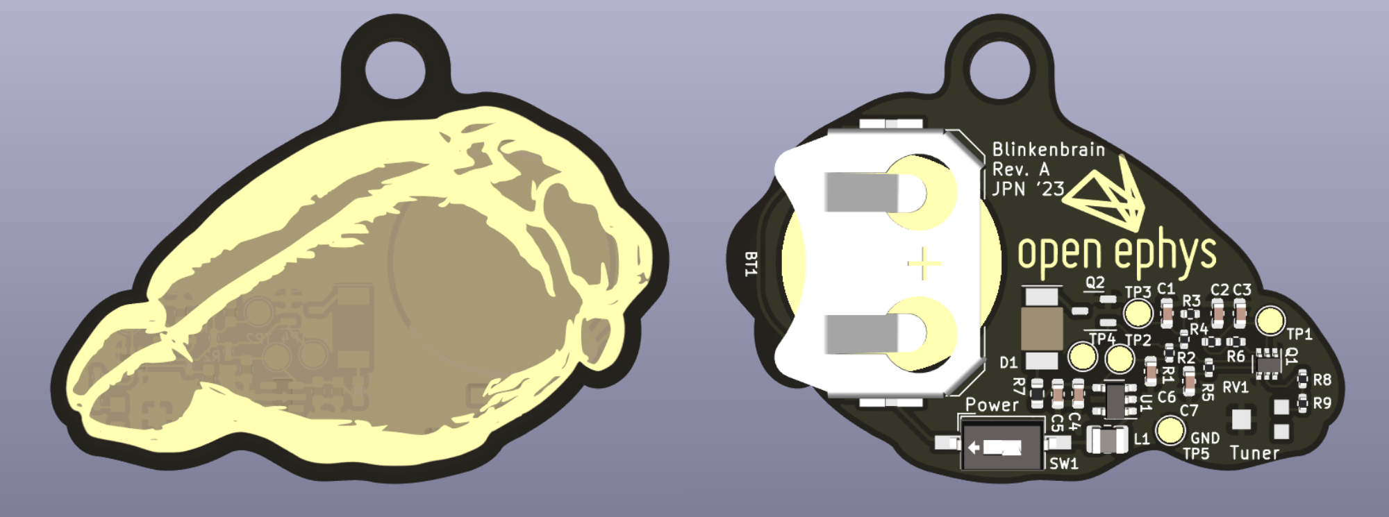
Mouse brain pendant with chaotic tendencies
Blinkenbrain panel is an open-source printed circuit board by open-ephys, from the open-ephys/blinkenbrain repository on GitHub. It is a 2-layer board of 300 × 320 mm with 600 parts on 16 nets, routed with 2,080 tracks and 0 vias.
It is built around the BC847BS, DFE252012P-2R2M=P2 and TC33X-2-104E, with the XZVG45WT-9 among its other parts. Its parts include 180 resistors, 140 capacitors, 40 ICs, 20 diodes and 20 transistors.


A mouse brain pendant with chaotic tendencies. It implements a variant of the circuit described in
Simple Two-Transistor Single-Supply Resistor–Capacitor Chaotic Oscillator
Lars Keuninckx, Guy Van der Sande, and Jan Danckaert
IEEE TRANSACTIONS ON CIRCUITS AND SYSTEMS—II: EXPRESS BRIEFS, VOL. 62, NO. 9, SEPTEMBER 2015
and uses its strange dynamics to blink a blinkenlight.
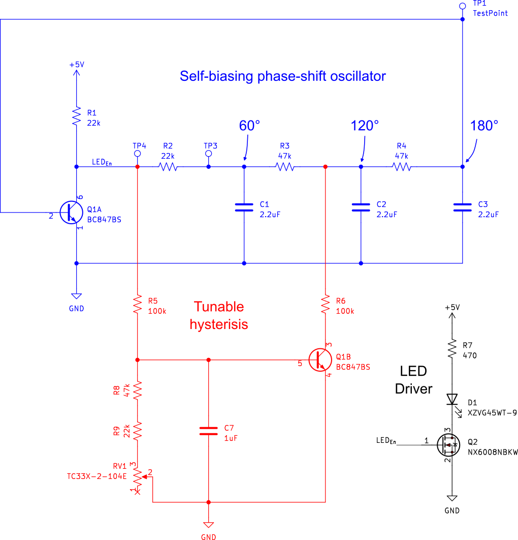
The circuit consists of a RC phase shift oscillator (blue) combined with what amounts to a tunable Schmitt trigger (red). The position of the trimpot (RV1) determines if the effect of the Schmitt trigger on the oscillator.
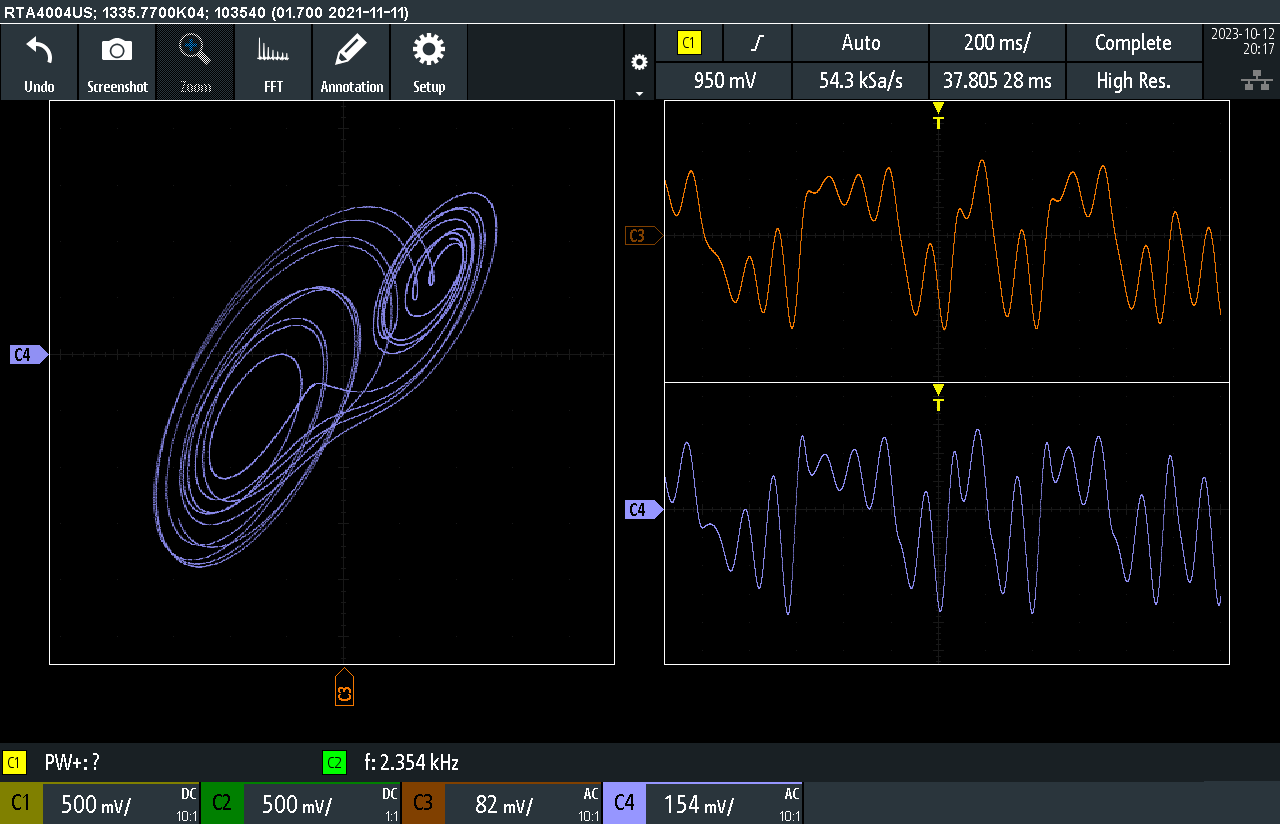
The gate of an N-channel MOSFET is tied to the collector of Q1A to drive the LED without influencing the circuit's dynamics. The following image shows VTP4 vs.VTP3 when RV1 is tuned to ~70kΩ.
"No Rights Reserved", CC0
| Qty | Value | Footprint | References |
|---|---|---|---|
| 100 | TestPoint | TestPoint:TestPoint_Pad_D2.0mm | TP1, TP1, TP1, TP1, TP1, TP1, TP1, TP1, TP1, TP1, TP1, TP1, TP1, TP1, TP1, TP1 +84 |
| 60 | 10uF | Capacitor_SMD:C_0603_1608Metric | C4, C4, C4, C4, C4, C4, C4, C4, C4, C4, C4, C4, C4, C4, C4, C4 +44 |
| 60 | 2.2uF | Capacitor_SMD:C_0603_1608Metric | C1, C1, C1, C1, C1, C1, C1, C1, C1, C1, C1, C1, C1, C1, C1, C1 +44 |
| 60 | 22k | Resistor_SMD:R_0603_1608Metric | R1, R1, R1, R1, R1, R1, R1, R1, R1, R1, R1, R1, R1, R1, R1, R1 +44 |
| 60 | 47k | Resistor_SMD:R_0402_1005Metric | R3, R3, R3, R3, R3, R3, R3, R3, R3, R3, R3, R3, R3, R3, R3, R3 +44 |
| 40 | 100k | Resistor_SMD:R_0402_1005Metric | R5, R5, R5, R5, R5, R5, R5, R5, R5, R5, R5, R5, R5, R5, R5, R5 +24 |
| 20 | 120 | Resistor_SMD:R_0603_1608Metric | R7, R7, R7, R7, R7, R7, R7, R7, R7, R7, R7, R7, R7, R7, R7, R7 +4 |
| 20 | 1uF | Capacitor_SMD:C_0603_1608Metric | C7, C7, C7, C7, C7, C7, C7, C7, C7, C7, C7, C7, C7, C7, C7, C7 +4 |
| 20 | 2.54-1P TPGT | Button_Switch_SMD:SW_DIP_SPSTx01_Slide_6.7x4.1mm_W8.61mm_P2.54mm_LowProfile | SW1, SW1, SW1, SW1, SW1, SW1, SW1, SW1, SW1, SW1, SW1, SW1, SW1, SW1, SW1, SW1 +4 |
| 20 | 3034 | open-ephys:KEYSTONE_3034_1x20mm | BT1, BT1, BT1, BT1, BT1, BT1, BT1, BT1, BT1, BT1, BT1, BT1, BT1, BT1, BT1, BT1 +4 |
| 20 | BC847BS | Package_TO_SOT_SMD:SOT-363_SC-70-6 | Q1, Q1, Q1, Q1, Q1, Q1, Q1, Q1, Q1, Q1, Q1, Q1, Q1, Q1, Q1, Q1 +4 |
| 20 | DFE252012P-2R2M=P2 | Inductor_SMD:L_1008_2520Metric | L1, L1, L1, L1, L1, L1, L1, L1, L1, L1, L1, L1, L1, L1, L1, L1 +4 |
| 20 | LMV321AIDCKR | Package_TO_SOT_SMD:SOT-353_SC-70-5 | U2, U2, U2, U2, U2, U2, U2, U2, U2, U2, U2, U2, U2, U2, U2, U2 +4 |
| 20 | LOGO | LOGO | G***, G***, G***, G***, G***, G***, G***, G***, G***, G***, G***, G***, G***, G***, G***, G*** +4 |
| 20 | TC33X-2-104E | open-ephys:BOURNS_TC33 | RV1, RV1, RV1, RV1, RV1, RV1, RV1, RV1, RV1, RV1, RV1, RV1, RV1, RV1, RV1, RV1 +4 |
| 20 | TPS613222ADBVR | Package_TO_SOT_SMD:SOT-23-5 | U1, U1, U1, U1, U1, U1, U1, U1, U1, U1, U1, U1, U1, U1, U1, U1 +4 |
| 20 | XZVG45WT-9 | open-ephys:SUNLED_PLCC2-INV | D1, D1, D1, D1, D1, D1, D1, D1, D1, D1, D1, D1, D1, D1, D1, D1 +4 |


test-gh-syncer2/Soldered-Mini-boost-converter-hardware-design
Hardware design, BOM, gerbers, 3D files and pinout for Mini_boost_converter designed by Soldered.


It measures 300 × 320 mm and has 2 copper layers, 1.6 mm thick.
600 parts, built around the BC847BS, DFE252012P-2R2M=P2, TC33X-2-104E and XZVG45WT-9. The full list of its parts is on this page, with links to each part's symbol and footprint where PCBKit's library has them.
From the open-ephys/blinkenbrain repository on GitHub, at the commit this page was made from: the board is pcb/blinkenbrain_panel.kicad_pcb and its schematic pcb/blinkenbrain.kicad_sch. PCBKit opens the board in the browser, with nothing to install.
Its repository states no licence, so its author keeps all rights: ask open-ephys before reusing the design.