
2 layers110.7 × 67.8 mm
Cyberdeck
awesomebrownies/cyberdeck
Deck Featuring: Controllers, shock cage, folding travel mode, and picatinny rails
38 parts2

 oddgrd/auge
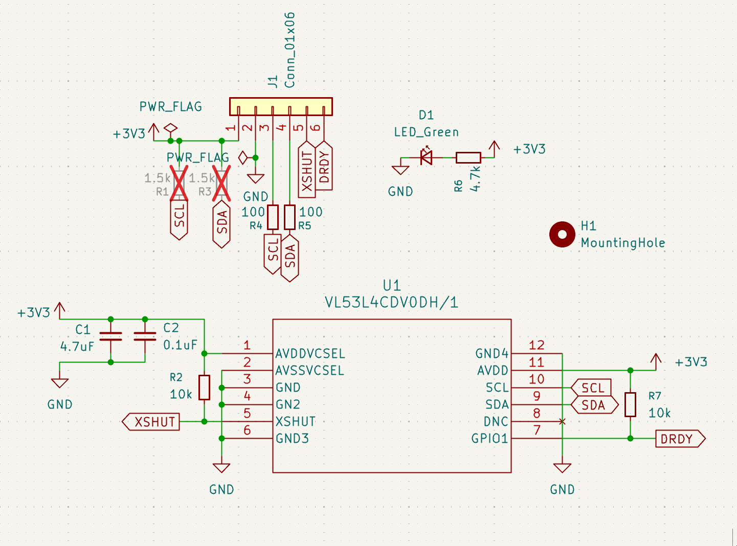
This repo contains the kicad PCB files, as well as libraries for footprints and symbols, for my [VL53L4CD][https://www.st.com/en/imaging-and-photonics-solutions/vl53l4cd.html] daughterboard.
Lidar pcb is an open-source printed circuit board by oddgrd, from the oddgrd/auge repository on GitHub. It is a 2-layer board of 17 × 14.5 mm with 16 parts on 10 nets, routed with 73 tracks and 11 vias.
It is built around the VL53L4CDV0DH/1. Its parts include 7 resistors, 2 capacitors, 1 IC, 1 diode and 1 connector.
This repo contains the kicad PCB files, as well as libraries for footprints and symbols, for my [VL53L4CD][https://www.st.com/en/imaging-and-photonics-solutions/vl53l4cd.html] daughterboard. It is also compatible with VL53L0X. It is largely designed to work with my Sumodd motherboard, but it could be used independently with some modification.
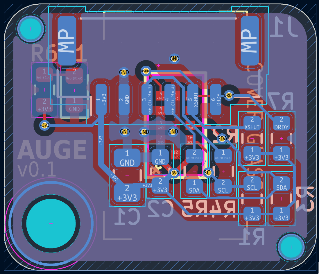
The board is two layers, 1mm thick, with a standard 1oz copper on each side:
Two tooling holes were added to opposite corners to meet JLCPCB assembly requirements. The schematic includes fields for LCSC part numbers, which are used in JLCPCB assembly.
All components are laid out as documented in the VL53L4CD datasheet, section 1.4. All SMD support components are 0603 imperial, except the 4.7uF cap, which is 0805. I could have gone smaller, but want to be able to make changes easily, when experimenting with I2C pullups and series resistors.
The area around the sensor on the top side is left clear, to make room for a potential cover glass in the future.
The Auge board is designed to work with my Sumodd motherboard, so while it has I2C pullup footprints, the resistors are DNP. If you want to use this board, you should either place pullups on the Auge board itself if you are only using one, or on the I2C bus of the board you connect it to if you are using several. Which resistors to use depends on your I2C bus capacitance, and which I2C clock speed you aim for. For more information on that, see section 1.4 in the VL53L4CD datasheet.
For reference, the Sumodd motherboard has low bus capacitance, so it places 1.5k pullups, along with the default 100 ohm series resistors on the Auge board. If you have higher bus capacitance, or if you don't want 1MHz I2C, you may want to change the series resistors too.
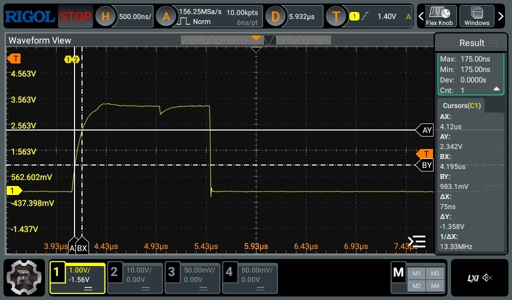
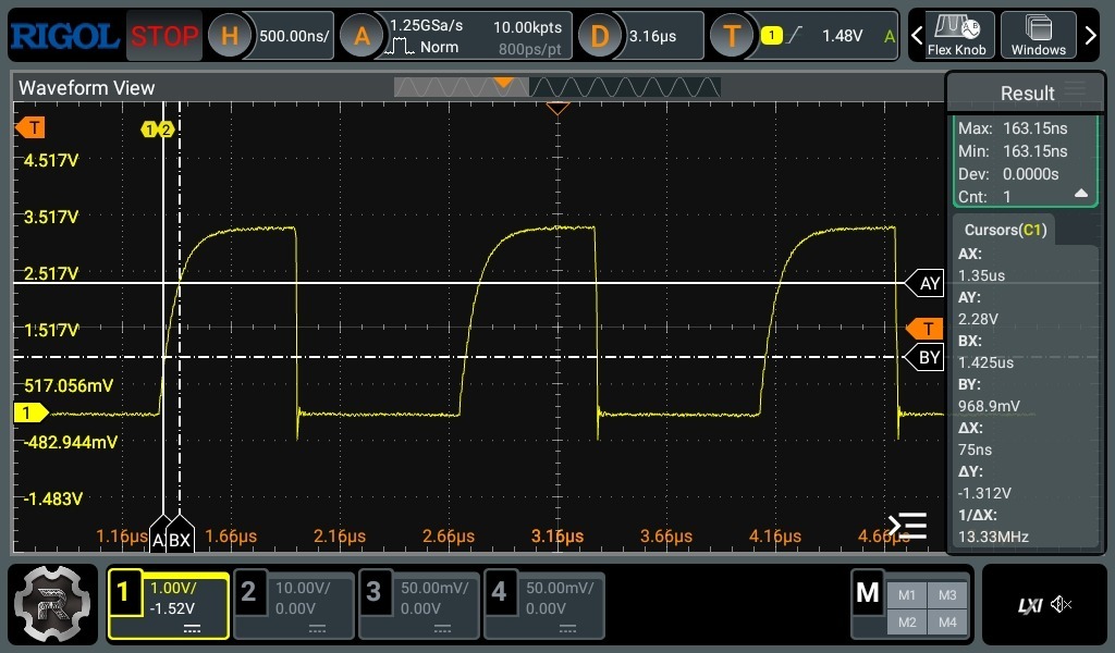
The first version of the board has been manufactured, and I scoped it to ensure it is working as expected. To achieve a 1MHz I2C speed at a bus capacitance of < 90 pF, I placed 100 ohm series resistors on each board, and 1.5k pullups on SDA and SCL on the motherboard, as described above.
The goal with the resistor configuration is to get SDA and SCL rise and fall times of max 120ns (table 5 in the VL53L4CD datasheet), to avoid communication errors, for example if SDA is supposed to be HIGH, but it hasn't risen past the receivers HIGH threshold by the time SCL crosses the HIGH threshold, and so the receiver may interpret the bit incorrectly.
Note that we measure the delta from 30% of VDD (the I2C pull-up voltage, 3.3V on Sumodd) to 70%, as this is the part that matters for digital logic. Anything over 70% will be considered HIGH, it doesn't matter how long it takes to get all the way to 100%. For more information on that, see section 3.1.2, as well as table 10 and 11 in the I2C spec.
We can see that the rise time for both SDA and SDL in this configuration is ~75ns, well within the limits, and the fall time is much faster.
SDA rise time on Sumodd motherboard (see cursor on the right):
SCL rise time on Sumodd motherboard (see cursor on the right):
| Qty | Value | Footprint | References |
|---|---|---|---|
| 2 | 1.5k | Resistor_SMD:R_0603_1608Metric | R1, R3 |
| 2 | 100 | Resistor_SMD:R_0603_1608Metric | R4, R5 |
| 2 | 10k | Resistor_SMD:R_0603_1608Metric | R2, R7 |
| 1 | 0.1uF | Capacitor_SMD:C_0603_1608Metric | C2 |
| 1 | 4.7k | Resistor_SMD:R_0603_1608Metric | R6 |
| 1 | 4.7uF | Capacitor_SMD:C_0805_2012Metric | C1 |
| 1 | CG-VL53L0X | CG-VL53L0X:CG-VL53L0X | CG |
| 1 | Conn_01x06 | Connector_JST:JST_GH_SM06B-GHS-TB_1x06-1MP_P1.25mm_Horizontal | J1 |
| 1 | LED_Green | LED_SMD:LED_0603_1608Metric | D1 |
| 1 | MountingHole | MountingHole:MountingHole_2.7mm_M2.5_ISO14580 | H1 |
| 1 | VL53L4CDV0DH/1 | VL53L4CDV0DH_1:LGA12_STM | U1 |
The 14 most common of 16 parts.
It measures 17 × 14.5 mm and has 2 copper layers, 1 mm thick.
16 parts, built around the VL53L4CDV0DH/1. The full list of its parts is on this page, with links to each part's symbol and footprint where PCBKit's library has them.
From the oddgrd/auge repository on GitHub, at the commit this page was made from: the board is lidar-pcb.kicad_pcb and its schematic lidar-pcb.kicad_sch. PCBKit opens the board in the browser, with nothing to install.
Its repository states no licence, so its author keeps all rights: ask oddgrd before reusing the design.
awesomebrownies/cyberdeck
Deck Featuring: Controllers, shock cage, folding travel mode, and picatinny rails

open-thngs/trap-a-rep-trigger
Device to detect passing creatures to trigger an external device like a DSLR camera


google/mozc-devices
Circuit diagrams and firmware source code for Gboard DIY keyboards

conorpp/u2f-zero
U2F USB token optimized for physical security, affordability, and style

rusefi/rusefi
rusefi - GPL internal combustion engine control unit