2 layers37 × 70.9 mm
Opendiag
maximus64/opendiag-hardware
OpenDIAG - Open Source OBD2 Interface (Hardware)
148 parts5CERN-OHL-S-2.0

 nxrmqlly/whitefox1
A devboard based on the Raspberry Pi RP2350B, with 47 GPIO, and microSD support
Whitefox is an open-source printed circuit board by nxrmqlly, from the nxrmqlly/whitefox repository on GitHub, published under the CERN-OHL-S-2.0 licence. It is a 4-layer board of 41 × 61.6 mm with 80 parts on 94 nets, routed with 1,063 tracks and 224 vias.
It is built around the W25Q128JVSIQ, AMS1117-3.3 and TP4056-42-ESOP8, with the USBLC6-2P6, WS2812B-2020 and 1N5819WS among its other parts. Its parts include 34 capacitors, 11 resistors, 11 diodes, 6 ICs and 6 connectors. It belongs with the microcontroller boards boards and the RP2350 boards of this library.


💥 very chonky!
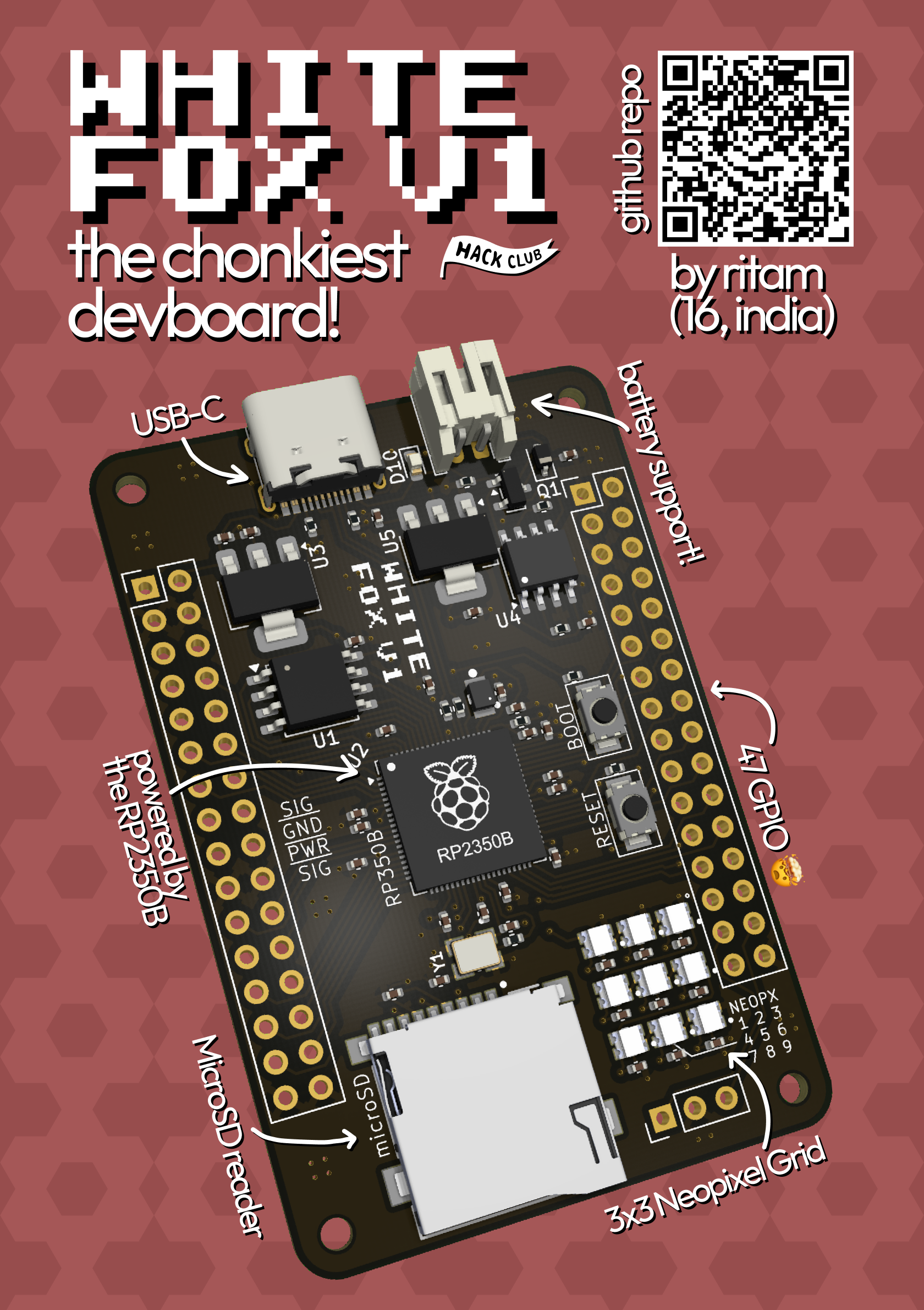
whitefox is a Raspberry Pi RP2350B based devboard with 47 exposed GPIO, a 3x3 neopixel grid, a charging circuit and a MicroSD card reader onboard! Some may even say that it is batteries included but sorry we don't include batteries :(
I wanted to have a go at making a devboard so I initially thought of using the RP2040 Chip but that thing is old now and very overused so here we are with the RP2040's successor, the RP2350! Most RP2350 boards (like the Raspberry Pi Pico 2) use the QFN-60 layout on the RP2350A chip and I haven't really seen devboards use the RP2350B, which is a QFN-80 chip, meaning it exposes the full power of the RP2350 in a bigger die.
The Schematic is a combination of very many different projects and the official and amazing
Hardware design with RP2350
The PCB is configured in a 4 layer stackup as follows (from the top): SIG / GND / PWR / SIG and includes copper pours on all layers except
the PWR layer (duh.)
Most components are SMD on top of the board, only the JST connector is through hole.
The PCB exposes two 2x16 standard 2.54 mm pitch header holes on both sides and an additional 1x3 2.54mm pitch connector as a debug header.
| What | Image |
|---|---|
| PCB | 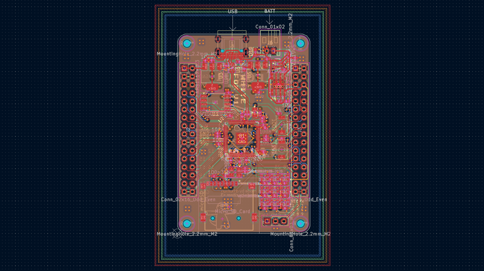 |
| Schematic | 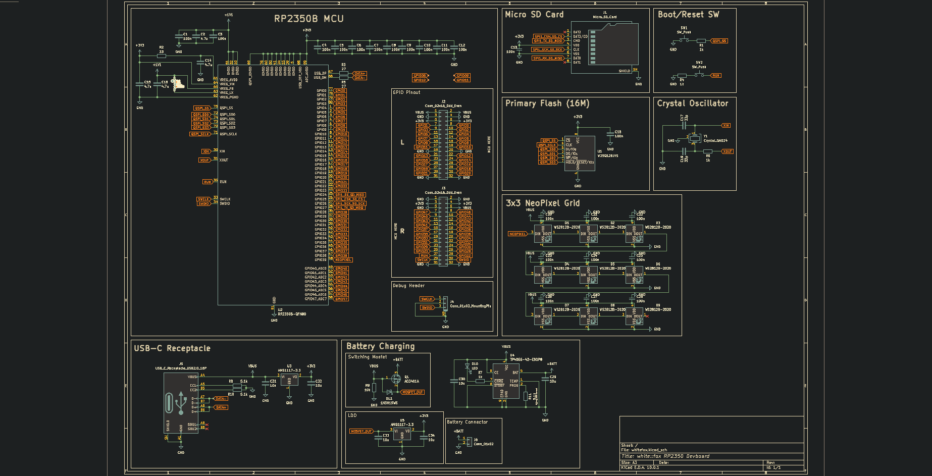 |
The PCB and Schematic are available in a high quality PDFs in Docs/
| Front | Back |
|---|---|
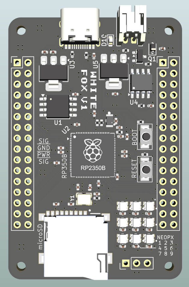 | 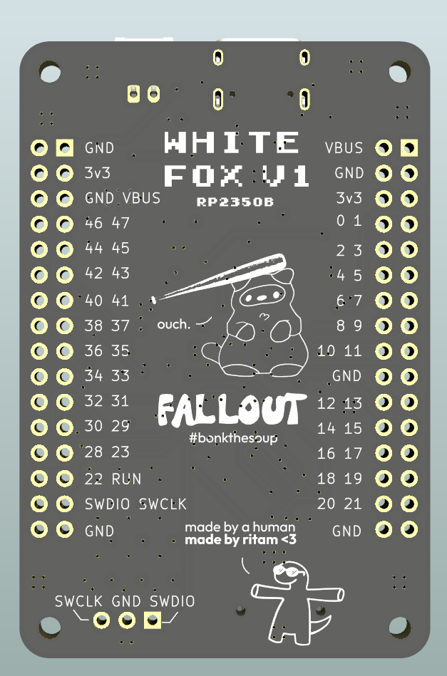 |
Lazy to type it here so...
The full BOM can be found at BOM/bom.csv!
There are 2 hard problems in computer science: cache invalidation, naming things, and off-by-1 errors.
-- Leon Bambrick
yeah that should be enough for an explanation.
Alternatively, you can preserve your sanity and get a PCBA service instead.
Grateful for:
The hardware (PCB) is licensed under CERN Open Hardware Licence Version 2 - Strongly Reciprocal which means, you're all-right to copy my work and use it in yours but you must disclose your source code and project files to opensource repositories if you include part of my work in yours. See LICENSE.
| Qty | Value | Footprint | References |
|---|---|---|---|
| 22 | 100n | Capacitor_SMD:C_0402_1005Metric | C1, C3, C10, C11, C12, C13, C18, C20, C21, C22, C23, C24, C25, C26, C27, C28 +6 |
| 9 | WS2812B-2020 | WS2812C-2020:LED_WS2812C-2020 | D1, D2, D3, D4, D5, D6, D7, D8, D9 |
| 6 | 10u | Capacitor_SMD:C_0402_1005Metric | C29, C30, C31, C32, C33, C34 |
| 4 | 1k | Resistor_SMD:R_0402_1005Metric | R1, R4, R6, R7 |
| 4 | 4.7u | Capacitor_SMD:C_0402_1005Metric | C2, C14, C15, C16 |
| 3 | 5.1k | Resistor_SMD:R_0402_1005Metric | R8, R10, R11 |
| 3 | LOGO | LOGO | G***, G***, G*** |
| 2 | 27 | Resistor_SMD:R_0402_1005Metric | R3, R5 |
| 2 | 33p | Capacitor_SMD:C_0402_1005Metric | C17, C19 |
| 2 | AMS1117-3.3 | Package_TO_SOT_SMD:SOT-223-3_TabPin2 | U3, U5 |
| 2 | Conn_02x16_Odd_Even | Connector_PinHeader_2.54mm:PinHeader_2x16_P2.54mm_Vertical | J2, J3 |
| 2 | SW_Push | TS-1088-TS-1088-ARXXX:TS-1088-ARXXX | SW1, SW2 |
| 1 | 10k | Resistor_SMD:R_0402_1005Metric | R9 |
| 1 | 1N5819WS | Diode_SMD:D_SOD-323 | D11 |
| 1 | 3.3u | jlc_kicad_footprint:IND-SMD_L2.0-W1.6_AOTA-B201610S3R3-101-T | L1 |
| 1 | 33 | Resistor_SMD:R_0402_1005Metric | R2 |
| 1 | AO3401A | Package_TO_SOT_SMD:SOT-23 | Q1 |
| 1 | Conn_01x02 | Connector_JST:JST_PH_S2B-PH-K_1x02_P2.00mm_Horizontal | J6 |
| 1 | Conn_01x03_MountingPin | Connector_PinHeader_2.54mm:PinHeader_1x03_P2.54mm_Vertical | J4 |
| 1 | Crystal_GND24 | XTAL_ABM8-272-T3:XTAL_ABM8-272-T3 | Y1 |
| 1 | LED | LED_SMD:LED_0603_1608Metric | D10 |
| 1 | Micro_SD_Card | TF-01A:TF-01A | J1 |
| 1 | RP2350B-QFN80 | Package_DFN_QFN:QFN-80-1EP_10x10mm_P0.4mm_EP3.4x3.4mm | U2 |
| 1 | TP4056-42-ESOP8 | Package_SO:SOIC-8-1EP_3.9x4.9mm_P1.27mm_EP2.41x3.3mm_ThermalVias | U4 |
| 1 | USBLC6-2P6 | Package_TO_SOT_SMD:SOT-666 | U6 |
| 1 | USB_C_Receptacle_USB2.0_16P | TYPE-C-31-M-12:TYPE-C-31-M-12 | J5 |
| 1 | W25Q128JVS | Package_SO:SOIC-8_5.3x5.3mm_P1.27mm | U1 |
The 76 most common of 80 parts.
maximus64/opendiag-hardware
OpenDIAG - Open Source OBD2 Interface (Hardware)


Queens-Rocket-Engineering-Team/Avionics-23-26
QRET Avionics hardware, firmware, and documentation for 2023 to 2025.


punkfab/pcb-corpus
235 real KiCad boards from open-source hardware repositories, prepared as a placement and routing benchmark
It measures 41 × 61.6 mm and has 4 copper layers, 1.6 mm thick.
80 parts, built around the W25Q128JVSIQ, AMS1117-3.3, TP4056-42-ESOP8 and USBLC6-2P6. The full list of its parts is on this page, with links to each part's symbol and footprint where PCBKit's library has them.
From the nxrmqlly/whitefox repository on GitHub, at the commit this page was made from: the board is PCB/whitefox.kicad_pcb and its schematic PCB/whitefox.kicad_sch. PCBKit opens the board in the browser, with nothing to install.
Its repository publishes it under the CERN-OHL-S-2.0 licence: you may reuse it on that licence's terms (keep the author's notice, and for a copyleft licence share your changes alike).