
4 layers161.1 × 82.9 mm

The purpose of Project Wrass is to develop the Wrass 1.
Uart is an open-source printed circuit board by nojan1, from the nojan1/project-wrass repository on GitHub. It is a 2-layer board of 133.3 × 85.2 mm with 54 parts on 138 nets, routed with 584 tracks and 38 vias.
It is built around the CD74HCT40105E, 74HCT193D and 74HCT165D, with the 74HCT595D, 74HCT00D and 74HCT08D among its other parts. Its parts include 21 capacitors, 18 ICs, 2 connectors, 1 resistor and 1 diode. It belongs with the interfaces and adapters boards of this library.


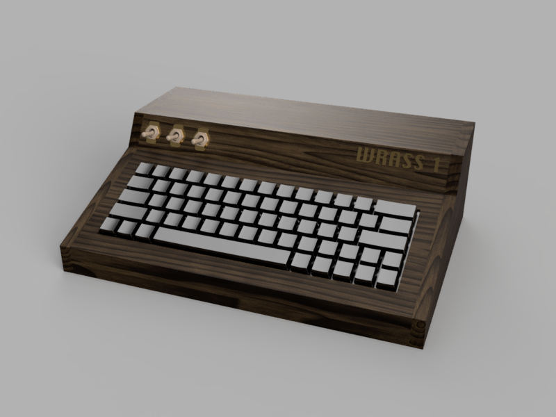
The purpose of Project Wrass is to develop the Wrass 1.
A 6502 based computer having the following specs.
Future specs:
- VGA output of 640x480 with 256 colors
- IO Card with W65C22 Vias and support for SPI
- Support for SD cards on IO card
- 8Mhz CPU clock speed
- Global scroll registers for video
- Sprites
- 3 channel sound synthesizer
The 16KB ROM is bankable using an external switch. This allows the computer to run "2 sets" of software.
The existing one is a simple homebrew "monitor" giving access to simple read, write and jump commands.
Future:
Support enhanced basic
| Qty | Value | Footprint | References |
|---|---|---|---|
| 18 | 0.1uf | Capacitor_THT:C_Rect_L7.2mm_W3.5mm_P5.00mm_FKS2_FKP2_MKS2_MKP2 | C1, C2, C6, C7, C10, C11, C12, C13, C14, C15, C16, C17, C18, C19, C20, C21 +2 |
| 8 | SolderJumper_2_Open | Jumper:SolderJumper-2_P1.3mm_Open_RoundedPad1.0x1.5mm | JP1, JP2, JP3, JP4, JP5, JP6, JP7, JP8 |
| 4 | CD74HCT40105E | Package_DIP:DIP-16_W7.62mm | U8, U9, U13, U14 |
| 3 | 74HCT193 | Package_DIP:DIP-16_W7.62mm | U3, U4, U17 |
| 2 | 22pf | Capacitor_THT:C_Rect_L7.2mm_W3.5mm_P5.00mm_FKS2_FKP2_MKS2_MKP2 | C4, C5 |
| 2 | 74HCT165 | Package_DIP:DIP-16_W7.62mm | U5, U6 |
| 2 | 74HCT595 | Package_DIP:DIP-16_W7.62mm | U11, U12 |
| 2 | MountingHole | MountingHole:MountingHole_2.5mm | H1, H2 |
| 1 | 1.8xx | Oscillator:Oscillator_DIP-14 | X1 |
| 1 | 100nf | Capacitor_THT:C_Radial_D5.0mm_H7.0mm_P2.00mm | C3 |
| 1 | 10K | Resistor_THT:R_Axial_DIN0207_L6.3mm_D2.5mm_P7.62mm_Horizontal | R1 |
| 1 | 1N4001 | Diode_THT:D_DO-41_SOD81_P10.16mm_Horizontal | D1 |
| 1 | 74HCT00 | Package_DIP:DIP-14_W7.62mm | U15 |
| 1 | 74HCT08 | Package_DIP:DIP-14_W7.62mm | U1 |
| 1 | 74HCT139 | Package_DIP:DIP-16_W7.62mm | U7 |
| 1 | 74HCT14 | Package_DIP:DIP-14_W7.62mm | U2 |
| 1 | 74HCT32 | Package_DIP:DIP-14_W7.62mm | U18 |
| 1 | 74HCT574 | Package_DIP:DIP-20_W7.62mm | U10 |
| 1 | 74HCT74 | Package_DIP:DIP-14_W10.16mm | U16 |
| 1 | Conn_02x25_Odd_Even | Connector_PinHeader_2.54mm:PinHeader_2x25_P2.54mm_Horizontal | J2 |
| 1 | UART | Connector_PinHeader_2.54mm:PinHeader_1x03_P2.54mm_Horizontal | J1 |


nojan1/project-wrass
The purpose of Project Wrass is to develop the Wrass 1.


nojan1/project-wrass
The purpose of Project Wrass is to develop the Wrass 1.


roberto314/EVA-1_Reproduction
Recreation of the very rare K-K Systems EVA-1 Display Adapter for the Epson HX-20 Computer

sittner/tinyfs
TinyFS is a minimalist filesystem designed for extremely constrained embedded systems. The initial reason to create this project was the attempt to build a filesystem that can run on a ZX81 without any additional…

leomil72/LM80C
A Z80-based homebrew computer withTMS9918, AY-3-8910, Z80 CTC, Z80 PIO, and Z80 SIO


MicroLind-Developers/microlind-hw
Hardware repository for the microlind project
It measures 133.3 × 85.2 mm and has 2 copper layers, 1.6 mm thick.
54 parts, built around the CD74HCT40105E, 74HCT193D, 74HCT165D and 74HCT595D. The full list of its parts is on this page, with links to each part's symbol and footprint where PCBKit's library has them.
From the nojan1/project-wrass repository on GitHub, at the commit this page was made from: the board is eda/uart-v1/uart.kicad_pcb and its schematic eda/all-in-one-smc/address-decode.kicad_sch. PCBKit opens the board in the browser, with nothing to install.
Its repository states no licence, so its author keeps all rights: ask nojan1 before reusing the design.