
2 layers99.7 × 99.7 mm
 nmahadevan12/MIS
Raspberry Pi multifunction instrumentation — digipot SAR ADC, ±12 V rail, function gens, KiCad Pi HAT (ECSE 2920).
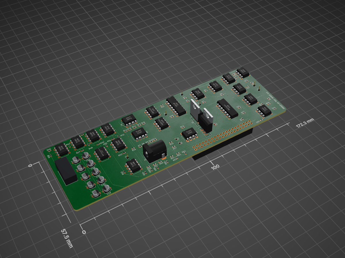
PCBDesign is an open-source printed circuit board by nmahadevan12, from the nmahadevan12/MIS repository on GitHub. It is a 4-layer board of 172.3 × 57.5 mm with 103 parts on 143 nets, routed with 801 tracks and 30 vias.
It is built around the TL081, LM339 and 1N4148WT, with the IRF5305PBF and IRFZ34N among its other parts. Its parts include 57 resistors, 21 ICs, 12 capacitors, 9 connectors and 2 diodes.


A portable, Raspberry Pi–powered electronic test bench that replaces six lab instruments — ohmmeter, voltmeter, DC reference, square/sine function generator, and frequency meter — with one integrated DAQ platform.


The Multifunction Instrumentation System integrates oscilloscopes, function generators, and multimeters into a single-board computer platform using the Raspberry Pi 4 as the central processing unit. Custom analog front-end circuits handle signal conditioning, comparison, and generation; Python firmware orchestrates measurement, waveform output, and a responsive menu-driven UI from a single application.
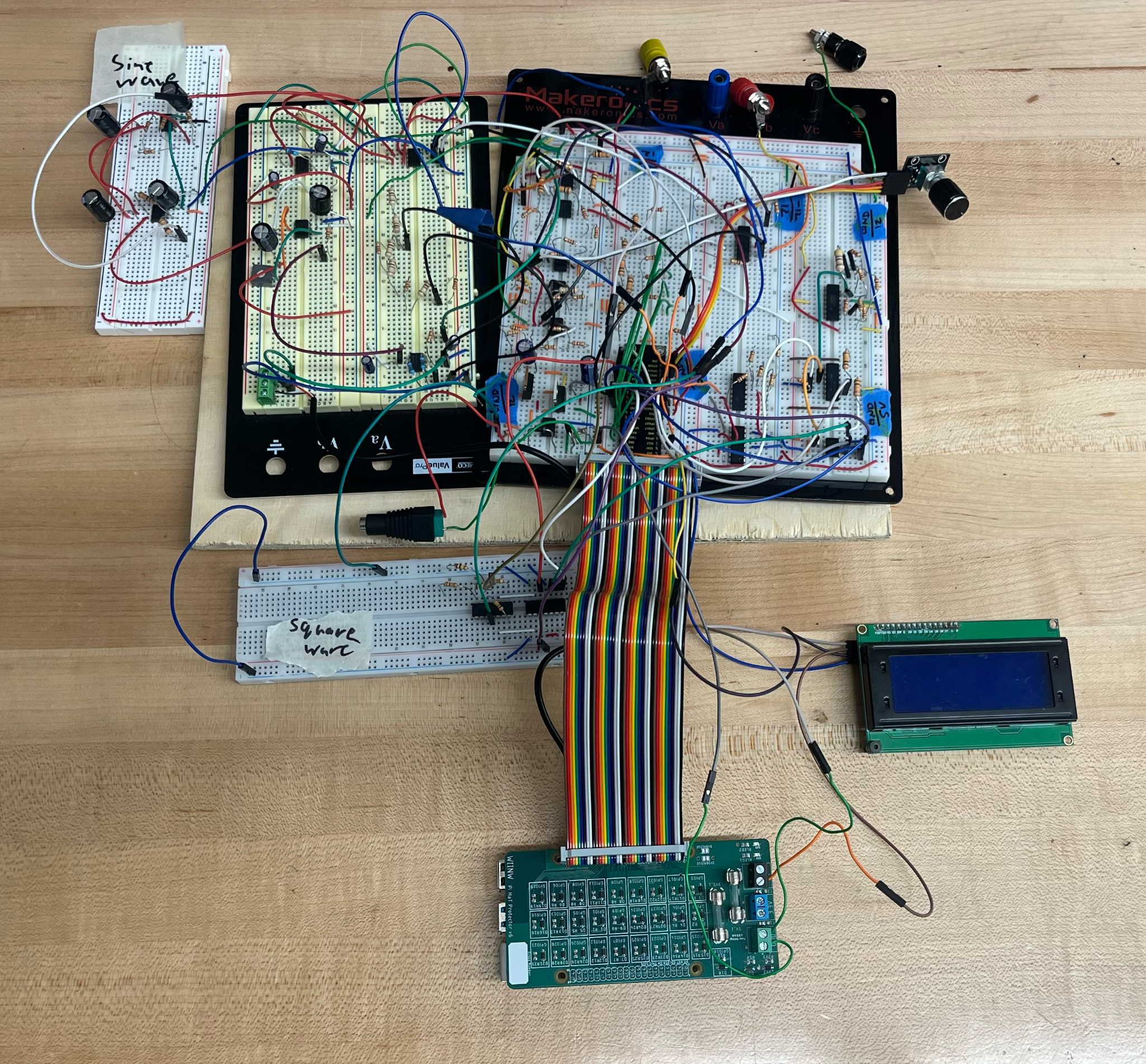
[!TIP] Documentation convention: Images show only schematics, photos, and oscilloscope captures. All objectives, theory, and figure captions are written as markdown text below each image.
| Controller | Raspberry Pi 4 (sole processor — no external MCU) |
| Interface | 20×4 I²C LCD + KY-040 rotary encoder with pushbutton |
| Analog front-end | TL084/TL081 op-amps, LM339 comparators, MCP4131/MCP4231 digipots |
| Power | 24 V DC input → ±12 V virtual-ground split-rail supply |
| Firmware | ~970 lines of Python — SAR measurement, hardware PWM, pigpio edge detection |
| PCB | 4-layer KiCad hierarchical design with Gerber manufacturing files |
Instrument design
System integration
PCB layout
| Category | Constraint |
|---|---|
| Software | All logic in Python; pigpio daemon for timing-critical PWM and edge detection |
| Controller | Raspberry Pi 4 only — no external microcontrollers |
| Digipots | Maximum of 4 digital potentiometers (MCP4131 ×3, MCP4231 ×1 dual-channel) |
| Power | All analog power derived from 24 V DC (LCD powered separately); Pi via USB-C |
| Mechanical | Pi Hat required — all GPIO routed through hat connector |
| Instrument | Range | Accuracy | Method |
|---|---|---|---|
| 🔵 Ohmmeter | 500 Ω – 10 kΩ | ±10% | GPIOs |
| 🟢 Voltmeter | −5 V to +5 V | ±0.2 V | GPIOs |
| 🟡 DC Reference | −5.00 V to +4.80 V (32 steps) | ±0.2 V | GPIOs |
| 🟠 Square Wave | 100 Hz – 10 kHz, ±10 V pk | ±0.1 V amplitude / ±1% freq | PWM |
| 🟣 Sine Wave | 1 – 10 kHz, 0 – 10 V pk | ±0.1 V amplitude / ±1% freq | Audio |
| 🔴 Frequency Meter | 1 – 10 kHz | ±1% | GPIOs |
flowchart LR
    subgraph UI["🖥️ User Interface"]
        LCD["20×4 I²C LCD"]
        ENC["Rotary Encoder"]
    end

    subgraph SW["🐍 Python Firmware"]
        MENU["Menu State Machine"]
        SAR["SAR Engine"]
        PWM["Hardware PWM"]
        FREQ["Edge Detection"]
    end

    subgraph HW["⚡ Analog Front-End"]
        PS["±12V Supply"]
        MEAS["Ohm / Volt"]
        GEN["Wave Gen"]
        DCREF["DC Ref"]
    end

    ENC --> MENU --> LCD
    MENU --> SAR & PWM & FREQ
    SAR & PWM & FREQ --> HW
    PS --> HW
Software is the core of the system — it links the user interface to hardware modules, converts raw comparator signals into resistance/voltage values, controls waveform timing, and keeps the LCD updated.
| Layer | Technology |
|---|---|
| OS | Raspberry Pi OS |
| Execution | Standalone Python script (Main Code/16.py) |
| GPIO / PWM | RPi.GPIO, pigpio (hardware PWM + µs edge timestamps) |
| SPI | spidev — MCP4131 / MCP4231 digital potentiometers |
| I²C | smbus2, RPLCD — 20×4 character LCD |
| UI input | gpiozero — rotary encoder + button callbacks |
The interface is a stack-based menu tree with automatic hardware cleanup on back-navigation. Measurement modes sample every 500 ms; the LCD refreshes on a 50 ms display flag with thread-safe writes.
To ensure a highly responsive user interface, the 500 ms hardware measurement routines run asynchronously or utilize non-blocking sleep intervals. This prevents the synchronous 8-bit SPI SAR sweeps from blocking encoder interrupt callbacks or delaying the 50 ms LCD UI refresh cycle.
while True:
    if display_needs_update → render_interface()
    if measurement_mode     → sample hardware every 500 ms
    if leaving_mode         → cleanup GPIO / stop waveforms
sleep(0.05)| Instrument | Key Implementation |
|---|---|
| Square wave | Hardware PWM GPIO 12 + MCP4231 amplitude/offset over SPI |
| Sine wave | Pi audio jack + speaker-test; MCP4131 amplitude (CS GPIO 17) |
| Ohmmeter | 8-iter SAR on MCP4131; R = R_known × (step / (128 − step)) |
| Voltmeter | SAR on GPIO 6; lookup table + linear interpolation |
| DC Reference | 5-bit R-2R on GPIO 14, 15, 18, 23, 24 |
| Frequency | pigpio edge callbacks GPIO 25; 100-period buffer, >2σ outlier reject |
[!IMPORTANT] All waveform and DC outputs automatically disable when leaving a menu — a built-in safety interlock.
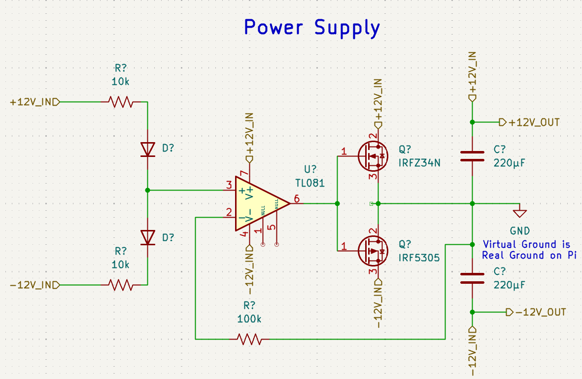
Figure 4.1.1: Power Supply Schematic
Objective: Split a +24 V DC input into symmetric +12 V and −12 V rails to power op-amps throughout the system. Rails must remain stable under varying load.
Theory of Operation: Virtual ground from a 24 V source. TL081 unity-gain follower at the 12 V midpoint drives IRFZ34N + IRF5305 push-pull stage. Virtual ground tied to Pi GND → +12 V above, −12 V below. The virtual ground node acts as the absolute 0 V reference point for all analog measurements. To prevent heavy analog return currents from injecting noise into the digital plane, the Raspberry Pi GND is tied to this virtual ground at a single star-ground point right at the power entry terminal.
Physical Integration: Breadboard; ±12 V via terminal blocks. GPIO: None — analog only.
| Test Condition | Negative Rail | Positive Rail | Current |
|---|---|---|---|
| Both loads connected | −12.04 V | +12.05 V | ~12 mA each |
| No load | −12.05 V | +12.06 V | — |
| Negative load only | 12.05 V | — | 12.10 mA |
| Positive load only | — | 12.06 V | 12.08 mA |
[!WARNING] MOSFETs run warm under heavy load. Observe electrolytic capacitor polarity on each rail.
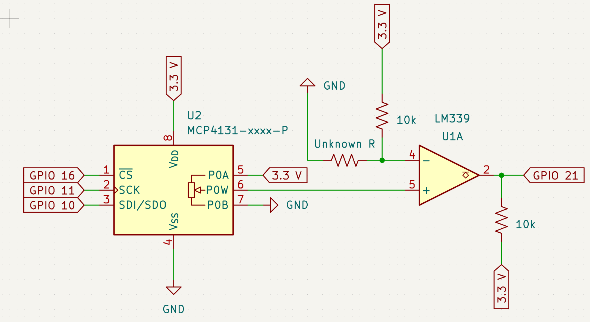
Figure 4.2.1: Ohmmeter Schematic
Objective: High-accuracy auto-ranging digital ohmmeter for 500 Ω to 10 kΩ.
Theory of Operation: Voltage divider with unknown resistor vs. 7-bit MCP4131 programmable reference. Successive approximation across 128 wiper steps; LM339 comparator on GPIO 21. LCD updates every 500 ms with ±10% tolerance. A fixed series current-limiting resistor (R_limit = 1 kΩ) is placed in series with the unknown device under test (DUT). This keeps the maximum current through the MCP4131 wiper well below its absolute maximum rating of 2.5 mA even when measuring low resistances down to 500 Ω.
| Signal | GPIO | Component Pin |
|---|---|---|
| Chip Select (CS) | 8 | MCP4131 Pin 1 |
| SPI Clock (SCK) | 11 | MCP4131 Pin 2 |
| SPI Data (SDI/SDO) | 10 | MCP4131 Pin 3 |
| Comparator Output | 21 | LM339 Output |
[!NOTE] SAR performance (8-bit search): Each iteration writes one MCP4131 wiper step over SPI (1 MHz, 2-byte frame ≈ 16 µs), waits 5 ms for the divider/comparator to settle (
sleep(0.005)), then reads GPIO 21. Eight bisection steps → ≈40 ms per resistance reading, well under the 500 ms LCD refresh cadence. Quantization is set by the 128-step digipot (7-bit effective range); resistance resolution is non-linear with step (R = R_known × step / (128 − step)) and tightest near the matched mid-scale point. Because the voltage-divider topology yields a non-linear resolution across the 128-step digipot, measurement precision peaks when the unknown resistance closely matches the internal reference (R_known). Near the outer bounds (500 Ω and 10 kΩ), step-size quantization broadens, which accounts for the specified worst-case ±10% tolerance.
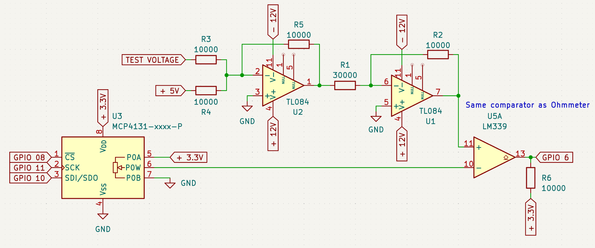
Figure 4.3.1: Voltmeter Schematic
Objective: Measure −5 V to +5 V at ±0.2 V accuracy. Dual-source: external input or internal DC reference verification.
Theory of Operation:
| Signal | GPIO | Component Pin |
|---|---|---|
| Chip Select (CS) | 8 | MCP4131 Pin 1 |
| SPI Clock (SCK) | 11 | MCP4131 Pin 2 |
| SPI Data (SDI/SDO) | 10 | MCP4131 Pin 3 |
| Comparator Output | 6 | LM339 Pin 13 |
[!NOTE] SAR performance (8-bit search): Same 8-iteration binary search as the ohmmeter — one SPI wiper write + 5 ms settle per step → ≈40 ms total sweep, safely below the 500 ms display refresh rate. The ±10 V input span maps to 128 comparator steps, giving a theoretical ≈78 mV/step (
10 V / 128 ≈ 78 mV); linear interpolation between calibrated lookup points improves display accuracy to ±0.2 V.
Calibration & Testing: Verified against reference multimeter across full range. SAR converges in 8 iterations. ±0.2 V accuracy; best precision near 0 V.
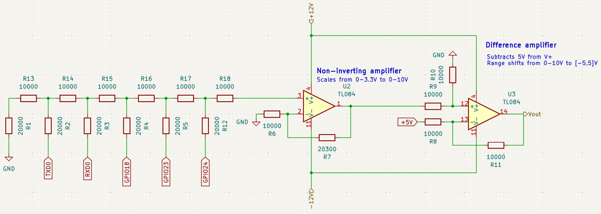
Figure 4.4.1: DC Ref Schematic
Objective: Programmable DC output −5 V to +5 V in 0.625 V steps (32 levels).
Calibration & Testing: Output verified across all 32 steps with a reference multimeter. Monotonic response confirmed from −5 V to +5 V.
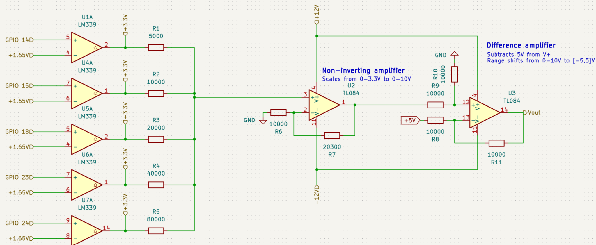
Figure 4.4.2: Previous DC Ref Schematic
Original binary-weighted DAC with per-GPIO comparator buffers suffered cross-loading. R-2R ladder maintains uniform 2R impedance regardless of bit pattern. The R-2R ladder ensures the digital pins always see a constant output impedance of R (or 2R depending on the node), preventing the voltage sag and non-monotonicity caused by varying pin source impedances in the previous binary-weighted layout.
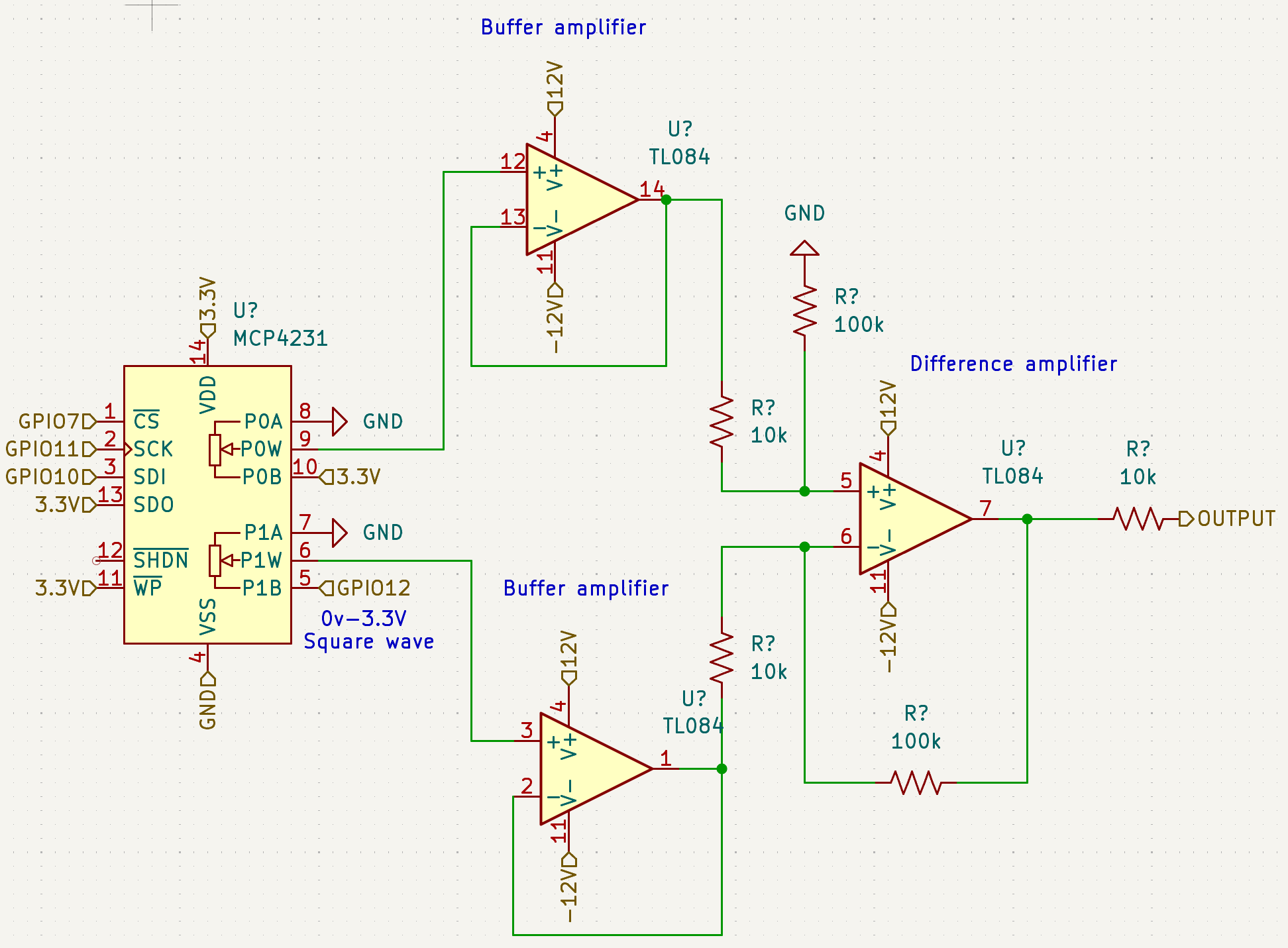
Figure 4.5.1: Square Wave Schematic
Objective: Variable square wave centered at 0 V, up to ±10 V, high-Z output for oscilloscope use.
Theory: Pi hardware PWM GPIO 12 → MCP4231 amplitude + offset → difference amplifier (gain 10) → ±10 V. The hardware PWM output from GPIO 12 passes through a dedicated RC low-pass filter stage to smooth high-frequency switching transients and stabilize the signal envelope before amplitude scaling, maintaining waveform integrity across the 100 Hz to 10 kHz band.
| Signal | GPIO | MCP4231 Pin |
|---|---|---|
| PWM Output | 12 | Ch1 Pin B |
| Chip Select | 7 | Pin 1 |
| SPI Clock | 11 | Pin 3 |
| SPI Data In | 10 | Pin 4 |
Calibration & Testing:
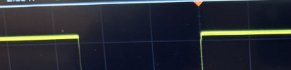
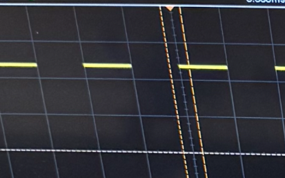
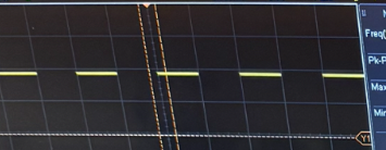
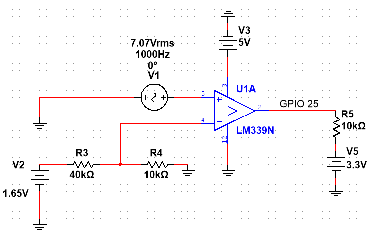
Figure 4.6.1: Sine Wave Measurement Schematic
Objective: Measure 0 V to +10 V sine input frequency from 1 kHz to 10 kHz.
Theory: LM339 threshold at +1.65 V → digital edges on GPIO 25 → f = 1/T. 100-period rolling buffer with >2σ outlier rejection.
pigpio edge architecture: On standard Linux (non-real-time), Python thread scheduling would jitter any bit-banged timing. The pigpio daemon sidesteps this by sampling GPIO transitions with hardware-level DMA, stamping each rising edge with a microsecond-accurate tick (pigpio.tickDiff) in a background buffer. The Python callback only appends period samples; compute_frequency() runs on the 500 ms UI loop, decoupling the timing-critical edge capture from GIL contention and kernel scheduling delay.
| Signal | GPIO | Component Pin |
|---|---|---|
| Comparator Output | 25 | LM339 Output |
| External Input | — | LM339 Non-Inverting Input |
| Reference (+1.65 V) | — | LM339 Inverting Input |
Calibration & Testing: ±2% tolerance across 1 – 10 kHz.
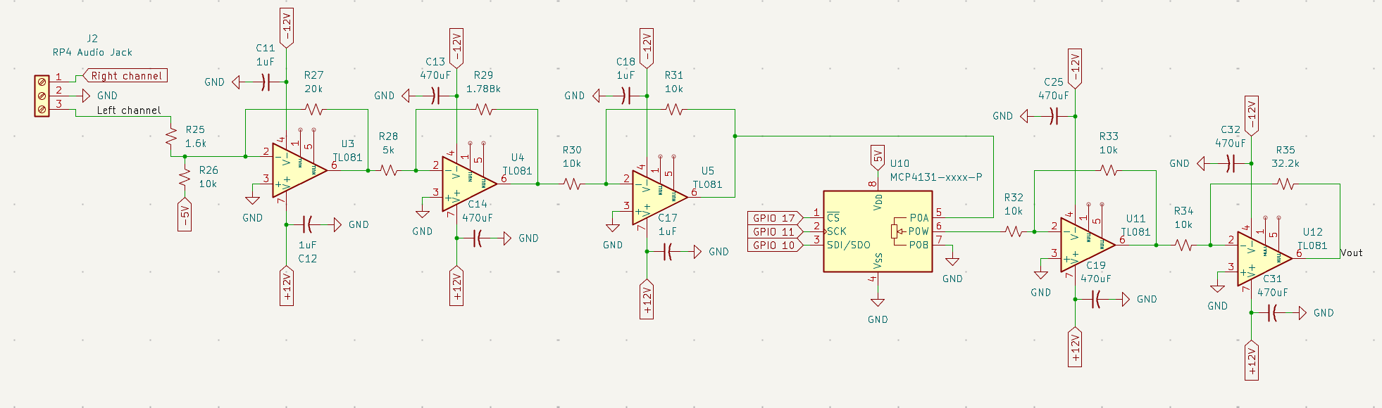
Objective: 0 – 10 V peak sine wave from 1 kHz to 10 kHz.
| Signal | GPIO | MCP4131 Pin |
|---|---|---|
| Chip Select | 17 | Pin 1 |
| SPI Clock | 11 | Pin 2 |
| SPI Data | 10 | Pin 3 |
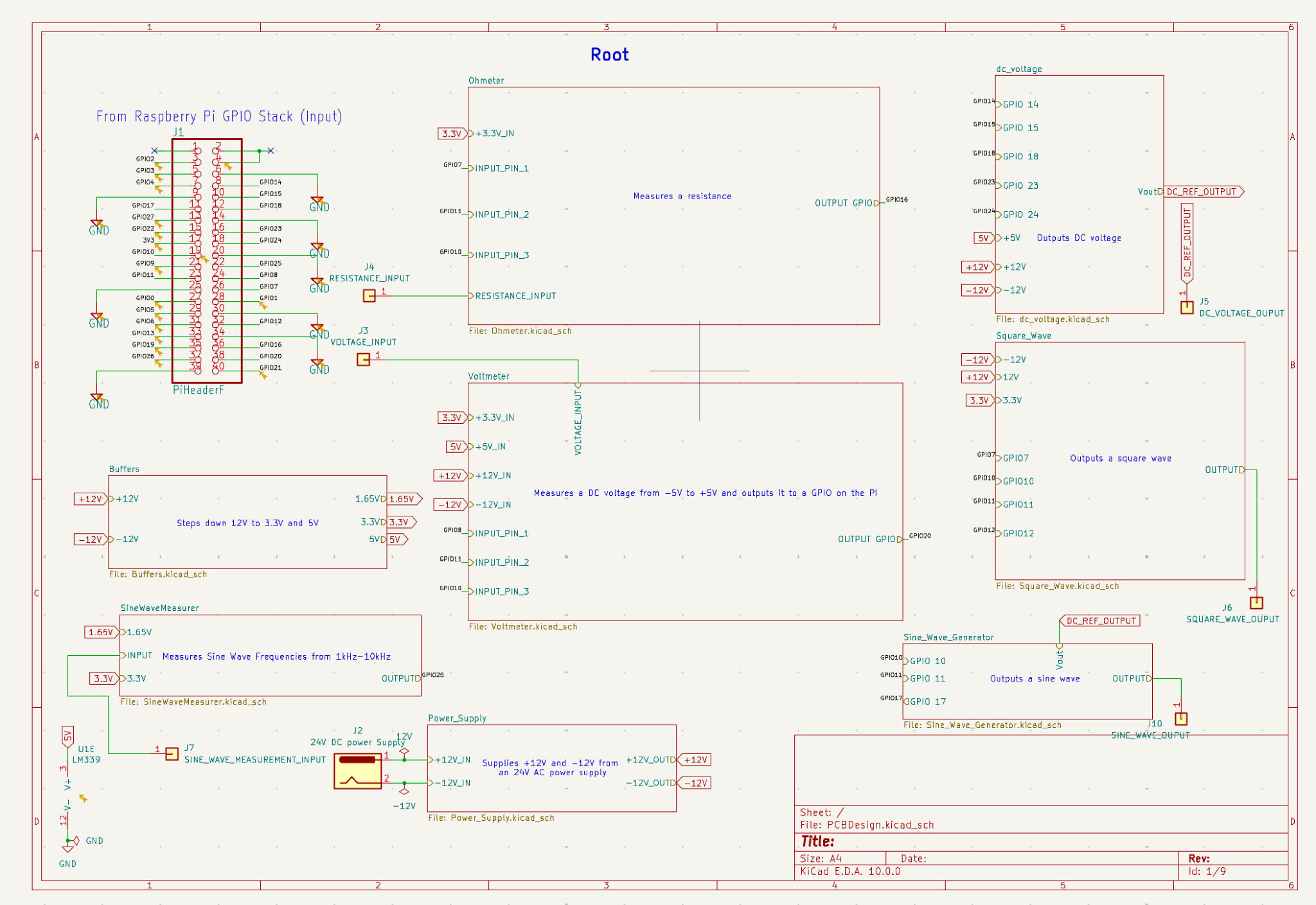
Figure 5.2.1: Final PCB Schematic
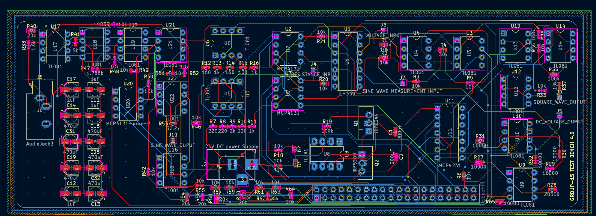
Figure 5.2.2: Final PCB Board
PCBDesign/ (designed, not manufactured)| GPIO | Signal | Component | Description |
|---|---|---|---|
| 2, 3 | SDA, SCL | LCD | I²C character display |
| 6 | Input | LM339 | Voltmeter comparator |
| 7 | SPI CS | MCP4231 | Square wave digipot |
| 8 | SPI CS | MCP4131 | Ohmmeter / voltmeter digipot |
| 10 | SPI MOSI | MCP4131/4231 | SPI data |
| 11 | SPI SCLK | MCP4131/4231 | SPI clock |
| 12 | HW PWM | — | Square wave output |
| 13, 19 | Input | KY-040 | Rotary encoder A/B |
| 14, 15, 18, 23, 24 | Output | R-2R ladder | DC reference (5-bit) |
| 17 | SPI CS | MCP4131 | Sine amplitude digipot |
| 21 | Input | LM339 | Ohmmeter comparator |
| 25 | Interrupt | LM339 | Frequency measurement |
| 26 | Input | KY-040 | Encoder button (3 s hold = back) |
[!NOTE] GPIO access requires
sudo. Thepigpiodaemon must be running for PWM and frequency measurement.
sudo apt update && sudo apt install -y python3-pip pigpio python3-pigpio alsa-utils
sudo systemctl enable --now pigpio
pip install -r requirements.txt
sudo python3 "Main Code/16.py"| Action | Control |
|---|---|
| Scroll | Rotate encoder |
| Select / confirm | Short press |
| Back / cancel | Hold 3 seconds |
| Edit value | Rotate in edit mode, press to confirm |
Power Pi via USB-C, analog circuits via 24 V DC. Wait ~20 s after boot.
[!TIP] Planned next steps: 12–16 bit external ADC, manufactured 4-layer PCB with ground planes, BNC/screw-terminal I/O, on-board regulators, active analog shielding.
|
Embedded Systems
Software Engineering
|
Analog Design
PCB / Systems
|
| Qty | Value | Footprint | References |
|---|---|---|---|
| 25 | 10k | Resistor_SMD:R_0603_1608Metric | R1, R2, R3, R5, R17, R18, R20, R21, R33, R34, R37, R39, R42, R46, R48, R49 +9 |
| 15 | TL081 | Package_DIP:DIP-8_W7.62mm | U3, U4, U5, U6, U9, U10, U12, U13, U14, U16, U17, U18, U19, U21, U22 |
| 7 | 20k | Resistor_SMD:R_0603_1608Metric | R40, R54, R56, R58, R60, R62, R64 |
| 6 | 10000 | Resistor_SMD:R_0603_1608Metric | R27, R29, R30, R31, R32, R65 |
| 6 | 470uF | Capacitor_SMD:CP_Elec_4x3 | C13, C14, C19, C25, C31, C32 |
| 4 | 1uF | Capacitor_SMD:CP_Elec_4x3 | C11, C12, C17, C18 |
| 3 | 100k | Resistor_SMD:R_0603_1608Metric | R19, R35, R36 |
| 3 | 1k | Resistor_SMD:R_0603_1608Metric | R11, R13, R16 |
| 3 | 220 | Resistor_SMD:R_0603_1608Metric | R7, R8, R10 |
| 2 | 160 | Resistor_SMD:R_0603_1608Metric | R12, R14 |
| 2 | 1N4148WT | Diode_SMD:D_SOD-523 | D1, D2 |
| 2 | 200µF | Capacitor_SMD:C_0603_1608Metric | C1, C2 |
| 2 | MCP4131 | Package_DIP:DIP-8_W7.62mm | U2, U7 |
| 1 | 1.6k | Resistor_SMD:R_0603_1608Metric | R38 |
| 1 | 1.788k | Resistor_SMD:R_0603_1608Metric | R47 |
| 1 | 100 | Resistor_SMD:R_0603_1608Metric | R15 |
| 1 | 20300 | Resistor_SMD:R_0603_1608Metric | R28 |
| 1 | 24V DC power Supply | Connector_BarrelJack:BarrelJack_Horizontal | J2 |
| 1 | 2k | Resistor_SMD:R_0603_1608Metric | R9 |
| 1 | 30k | Resistor_SMD:R_0603_1608Metric | R4 |
| 1 | 32.2k | Resistor_SMD:R_0603_1608Metric | R53 |
| 1 | 5k | Resistor_SMD:R_0603_1608Metric | R41 |
| 1 | AudioJack3 | Connector_Audio:Jack_3.5mm_CUI_SJ1-3533NG_Horizontal | J8 |
| 1 | DC_VOLTAGE_OUPUT | Connector_PinHeader_1.00mm:PinHeader_1x01_P1.00mm_Vertical | J5 |
| 1 | IRF5305 | Package_TO_SOT_THT:TO-220-3_Vertical | Q2 |
| 1 | IRFZ34N | Package_TO_SOT_THT:TO-220-3_Vertical | Q1 |
| 1 | LM339 | Package_DIP:DIP-14_W7.62mm | U1 |
| 1 | MCP4131-xxxx-P | Package_DIP:DIP-8_W7.62mm | U20 |
| 1 | MCP4231 | Package_DIP:DIP-14_W7.62mm | U11 |
| 1 | PiHeaderF | Connector_PinSocket_2.54mm:PinSocket_2x20_P2.54mm_Vertical | J1 |
| 1 | RESISTANCE_INPUT | Connector_PinHeader_1.00mm:PinHeader_1x01_P1.00mm_Vertical | J4 |
| 1 | SINE_WAVE_MEASUREMENT_INPUT | Connector_PinHeader_1.00mm:PinHeader_1x01_P1.00mm_Vertical | J7 |
| 1 | SINE_WAVE_OUPUT | Connector_PinHeader_1.00mm:PinHeader_1x01_P1.00mm_Vertical | J10 |
| 1 | SQUARE_WAVE_OUPUT | Connector_PinHeader_1.00mm:PinHeader_1x01_P1.00mm_Vertical | J6 |
| 1 | TL081 | Package_DIP:DIP-8_W7.62mm_LongPads | U8 |
| 1 | VOLTAGE_INPUT | Connector_PinHeader_1.00mm:PinHeader_1x01_P1.00mm_Vertical | J3 |
It measures 172.3 × 57.5 mm and has 4 copper layers, 1.6 mm thick.
103 parts, built around the TL081, LM339, 1N4148WT and IRF5305PBF. The full list of its parts is on this page, with links to each part's symbol and footprint where PCBKit's library has them.
From the nmahadevan12/MIS repository on GitHub, at the commit this page was made from: the board is Individual Components/8 - PCB Design/PCBDesign/PCBDesign.kicad_pcb and its schematic Individual Components/1 - Power Supply/Final_Power_Supply.kicad_sch. PCBKit opens the board in the browser, with nothing to install.
Its repository states no licence, so its author keeps all rights: ask nmahadevan12 before reusing the design.


AndrewPrimi/Group-5
This repository is used to store coursework, scripts, and supporting materials for our electronics and embedded systems projects throughout the semester.


edgranzella/Placa-de-Corte-TX
Circuito Impreso de la plaquetita de Corte TX que va apilada sobre el Arduino Nano de la placa Controladora de Fuentes y Carga.

Jonny999999/throttle-tune
onversion of an old gasoline lawn tractor to an electric vehicle