My KiCad learning path: fully documented PCB projects from a simple LED board to advanced designs, with schematics, layouts, Gerbers, calculations and verification reports.
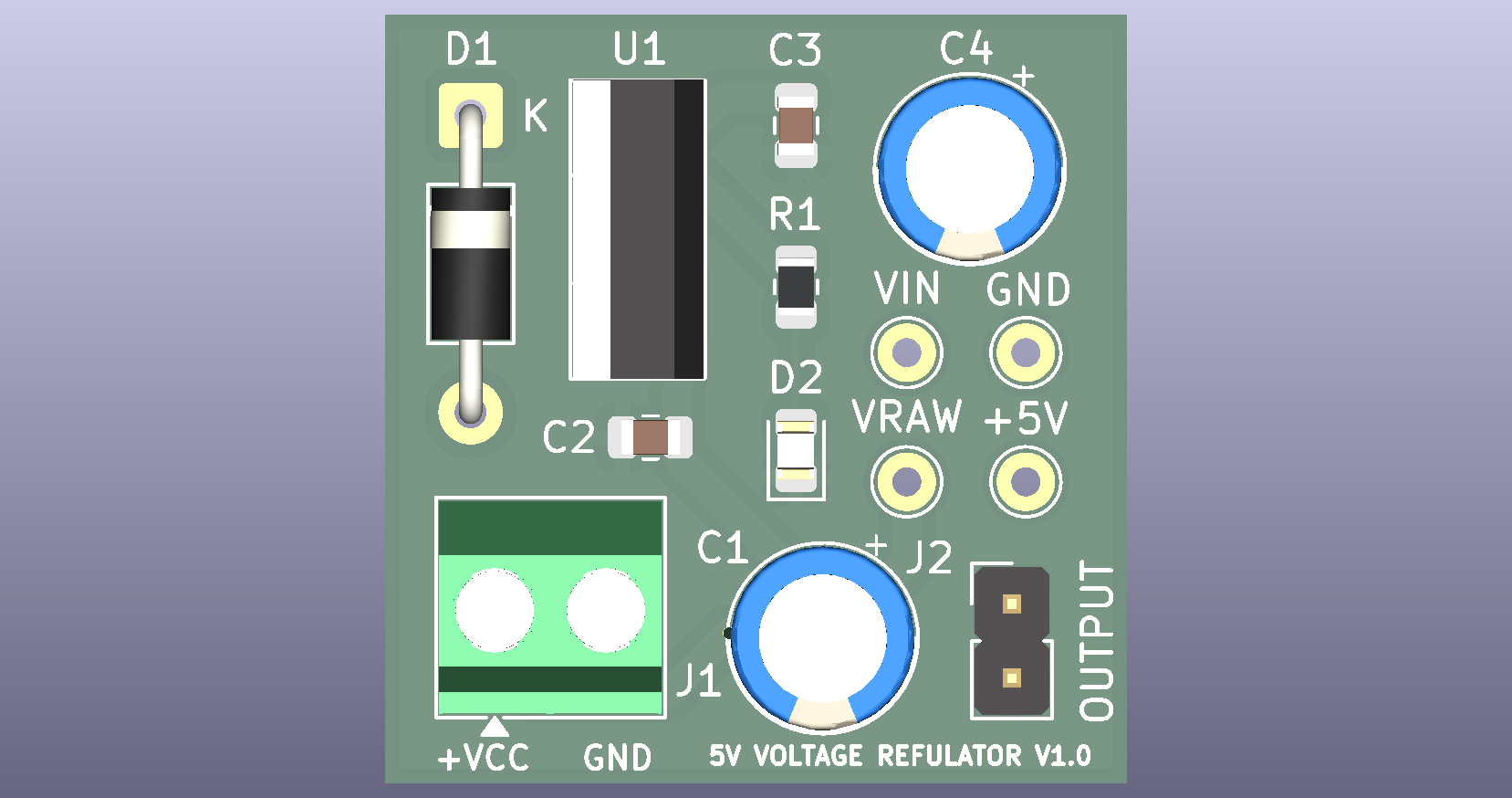
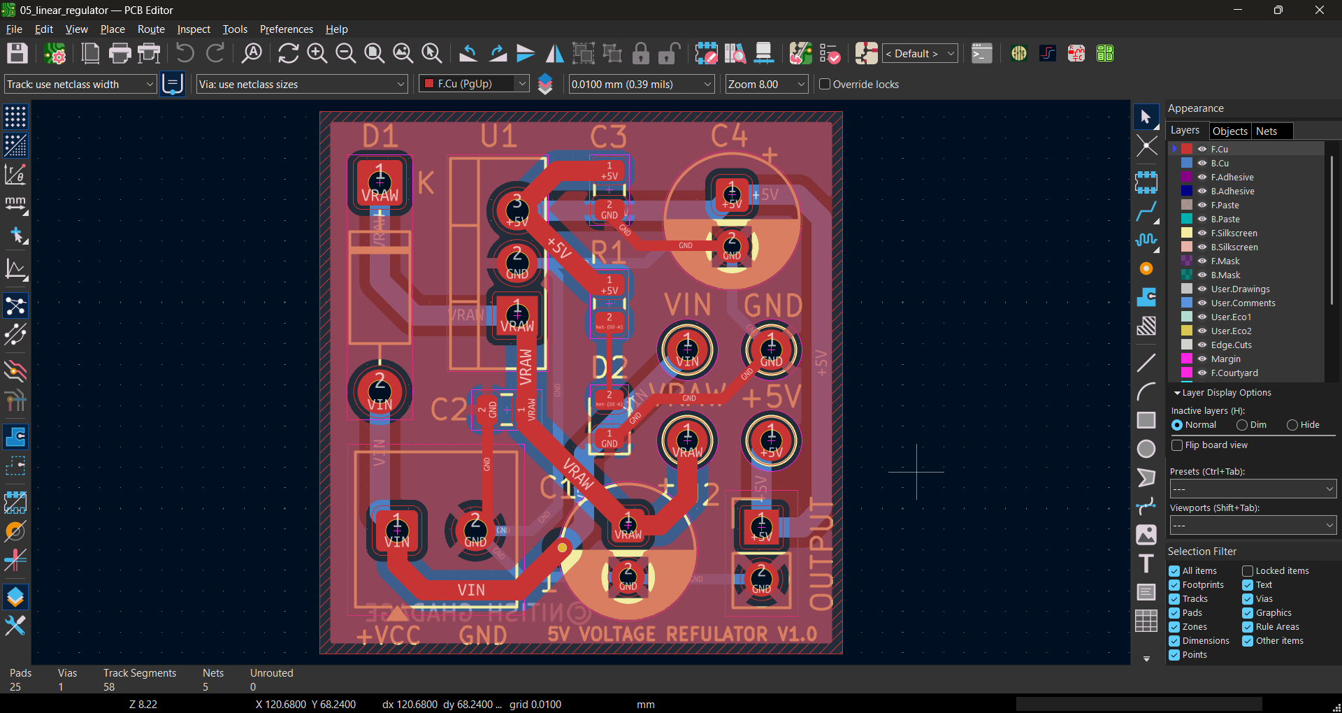
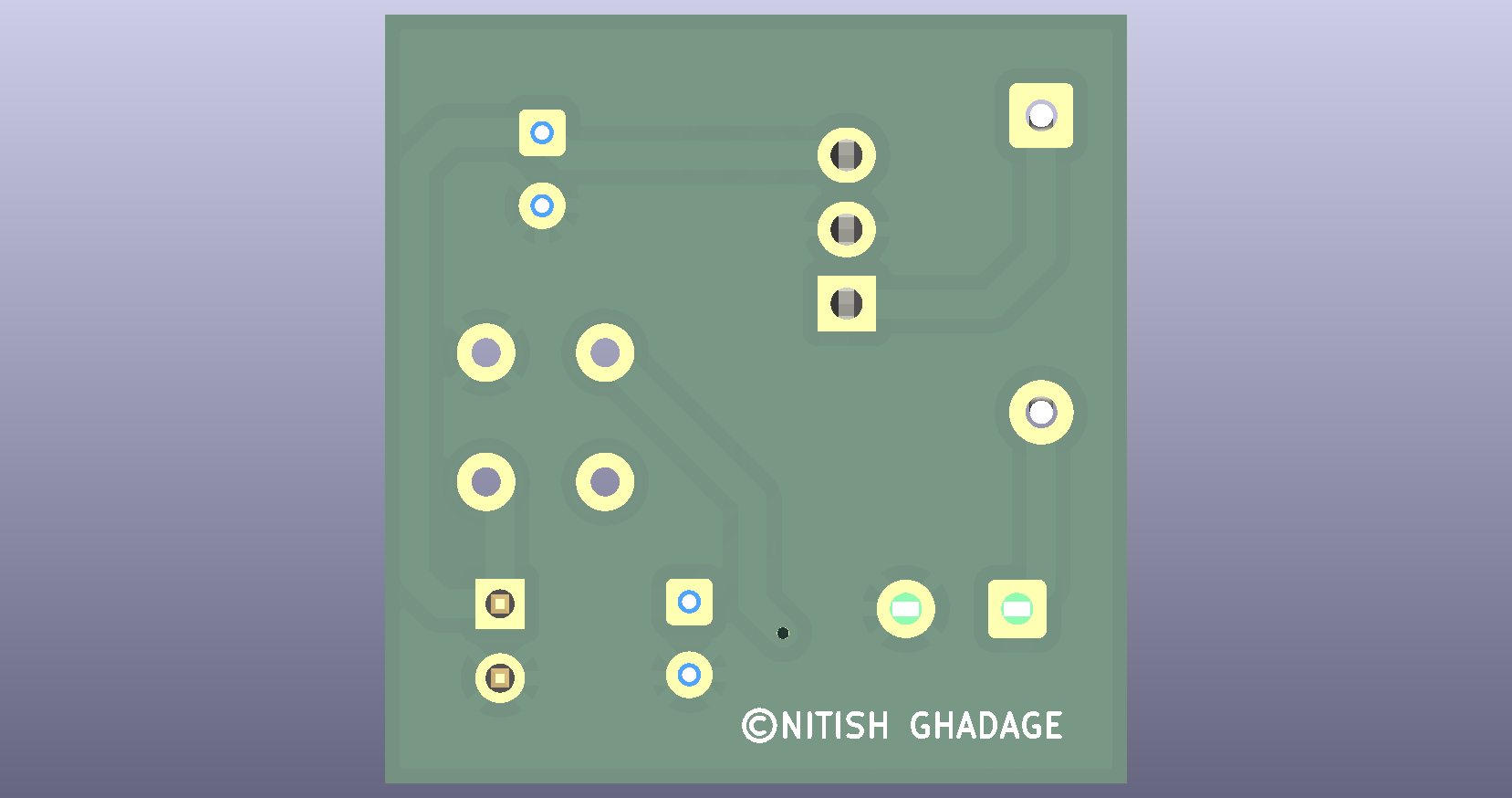
05 linear regulator is an open-source printed circuit board by nitu2126, from the nitu2126/kicad-learning-path repository on GitHub, published under the MIT licence. It is a 2-layer board of 25.4 × 26.3 mm with 14 parts on 5 nets, routed with 58 tracks and 1 via.
It is built around the L7805. Its parts include 4 capacitors, 2 diodes, 2 connectors, 1 resistor and 1 IC. It belongs with the power boards of this library.
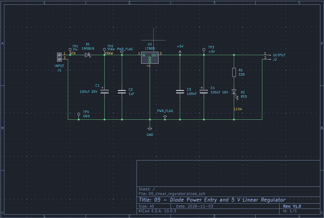
A 9 V battery or 7.6 V to 12 V DC supply turned into a clean 5 V rail: a Schottky diode against reverse connection, an L7805 linear regulator, input and output capacitors, a power LED and four test points.
Project 5 of my KiCad learning path: reverse-polarity protection, the linear regulator, capacitors that keep it stable, and heat.
Every earlier board assumed a clean 5 V supply. This board makes one. Real power sources are not clean: batteries sag, bench supplies are set too high, and people plug them in backwards. This board handles all three.
Section
Parts
What it demonstrates
Power entry
J1, D1
A series Schottky diode blocks a reversed connection, at the cost of a small voltage drop
Regulation
U1
A linear regulator turns any input from 7.6 V to 12 V into a steady 5 V, burning the difference as heat
Capacitors
C1 to C4
Bulk and high-frequency capacitors on the input and output
Indicator
R1, D2
A power LED that also provides the regulator's minimum load
Measurement
TP1 to TP4
Probe points before the diode, after the diode, at the output, and ground
New ideas compared with Project 4:
Reverse-polarity protection and the cost of a diode drop
Linear regulation, dropout voltage and efficiency
Heat: power dissipation, thermal resistance, junction temperature and heatsinks
Electrolytic and ceramic capacitors working together, and electrolytic polarity
The regulator's minimum load current
A wider net class (1.0 mm) for supply tracks
A voltage and power budget in the documentation
The full engineering write-up (theory, derivations, thermal analysis, KiCad configuration, layout rules, test procedure) is in docs/DESIGN_NOTES.md.
Key specifications
Parameter
Value
Input voltage
7.6 V to 12 V DC (9 V battery nominal), at screw terminal J1
Reverse-polarity protection
1N5819 Schottky, blocks up to 40 V in reverse
Output voltage
5 V, within 4.75 V to 5.25 V over all line, load and temperature conditions (datasheet)
Output current, free air
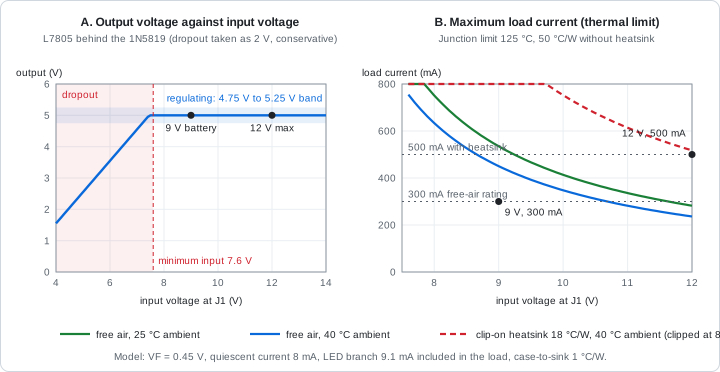
300 mA with up to 10 V input at 40 °C ambient
Output current, with heatsink
500 mA with up to 12 V input and a clip-on heatsink of 18 °C/W or better
Minimum load
5 mA, met by the power LED (9.1 mA)
Regulator heat
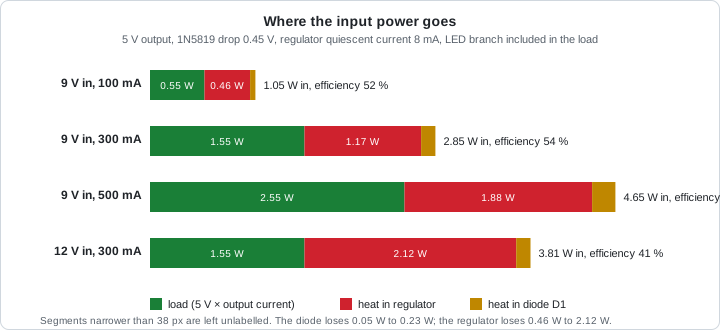
1.17 W at 9 V in and 300 mA out (junction 83 °C at 25 °C ambient)
Efficiency
54 % at 9 V in and 300 mA out, 41 % at 12 V in and 300 mA out
The output stays at 5 V while the input is high enough. Below about 7.6 V at J1 the regulator is in dropout and the output falls with the input
B. Maximum load against input
The higher the input voltage, the more heat the regulator must burn for the same current, so the allowed current falls. A heatsink raises the limit
Where the power goes
A linear regulator wastes the difference between input and output as heat. From 9 V to 5 V it can never be better than 56 % efficient, and from 12 V to 5 V never better than 42 %. At 9 V and 300 mA the regulator burns 1.17 W, while the load receives 1.55 W.
Reverse polarity. With the supply connected correctly, D1 conducts and drops about 0.45 V. If the supply is reversed, D1 is reverse-biased and blocks it, so nothing downstream sees a negative voltage.
Input capacitors.C1 (100 µF) is a reservoir that supplies sudden current demands. C2 (1 µF ceramic) sits at the regulator's input pin and handles fast changes. The datasheet asks for at least 0.33 µF at the input, with the shortest possible leads.
Regulation.U1 compares its output with an internal reference and adjusts an internal pass transistor to hold 5 V. The pass transistor drops the surplus voltage multiplied by the current, and that power becomes heat.
Output capacitors.C3 (100 nF) and C4 (100 µF) improve the response to load changes. The L7805 is stable without an output capacitor, but the datasheet notes that one improves transient response.
Minimum load. The regulator needs at least 5 mA of load to regulate properly. R1 and the power LED draw 9.1 mA, so it is always satisfied.
The metal tab of the TO-220 package is connected to ground (pin 2). It is the part that carries heat to a heatsink.
Design calculations (summary)
Minimum input voltage. The regulator needs its input to be at least 7 V (the datasheet's lowest test condition, equal to 5 V plus the 2 V dropout), and the diode takes up to 0.6 V:
Open 05-linear-regulator/05_linear_regulator.kicad_pro in KiCad. The project uses only the standard KiCad libraries.
Rebuild the manufacturing files
Open the PCB editor and run Inspect → Design Rules Checker. It should report 0 errors.
Open File → Fabrication Outputs → Gerbers and Generate Drill Files. The exact settings are listed in docs/DESIGN_NOTES.md.
Zip the output folder.
Order the PCB
Upload fabrication/05_linear_regulator_gerbers.zip to a PCB fabricator. Suggested options for a low-cost fab: 2 layers, 1.6 mm, 1 oz copper, HASL finish.
Testing
Safety first: the regulator gets hot (about 77 °C at its case when delivering 300 mA from 9 V) and the test load resistors get hot too. Step-by-step measurements, expected values, test loads and a troubleshooting table are in docs/DESIGN_NOTES.md. In short: test the reversed connection first with a current-limited supply, then apply 9 V and check TP2 (about 8.5 V) and TP3 (about 5.0 V), then load the output step by step.
My KiCad learning path: fully documented PCB projects from a simple LED board to advanced designs, with schematics, layouts, Gerbers, calculations and verification reports.
My KiCad learning path: fully documented PCB projects from a simple LED board to advanced designs, with schematics, layouts, Gerbers, calculations and verification reports.
My KiCad learning path: fully documented PCB projects from a simple LED board to advanced designs, with schematics, layouts, Gerbers, calculations and verification reports.
My KiCad learning path: fully documented PCB projects from a simple LED board to advanced designs, with schematics, layouts, Gerbers, calculations and verification reports.
An Open Source HardWare (OSHW) recreation of the 1993 toploading NES motherboard (Also known as NES-101)
84 parts94
Questions
How big is the 05 linear regulator PCB?
It measures 25.4 × 26.3 mm and has 2 copper layers, 1.6 mm thick.
What parts does the 05 linear regulator use?
14 parts, built around the L7805. The full list of its parts is on this page, with links to each part's symbol and footprint where PCBKit's library has them.
Where can I download the 05 linear regulator KiCad files?
From the nitu2126/kicad-learning-path repository on GitHub, at the commit this page was made from: the board is 05-linear-regulator/05_linear_regulator.kicad_pcb and its schematic 01-led-button/01_led_button.kicad_sch. PCBKit opens the board in the browser, with nothing to install.
Can I use the 05 linear regulator design in my own project?
Its repository publishes it under the MIT licence: you may reuse it on that licence's terms (keep the author's notice, and for a copyleft licence share your changes alike).