2 layers137.3 × 46.2 mm

 nict41/crossover
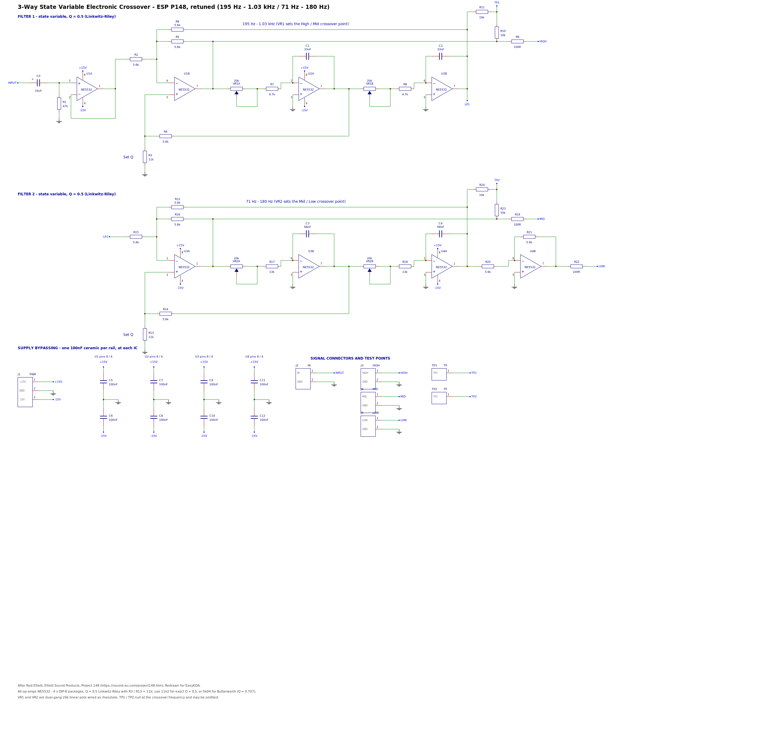
An EasyEDA-importable schematic for the 3-way state variable electronic crossover from Elliott Sound Products Project 148 ( ), redrawn from Figure 2.
Esp p148-3way crossover retuned quad smd is an open-source printed circuit board by nict41, from the nict41/crossover repository on GitHub. It is a 4-layer board of 149.6 × 63.5 mm with 90 parts on 64 nets.
It is built around the MC33079D, 1N4148W and MMBFJ112, with the TP1 among its other parts. Its parts include 40 resistors, 19 capacitors, 6 connectors, 4 diodes and 3 ICs.


An EasyEDA-importable schematic for the 3-way state variable electronic crossover from Elliott Sound Products Project 148 (https://sound-au.com/project148.htm), redrawn from Figure 2.
Two cascaded 2nd-order state variable filters, 12 dB/octave, with continuously variable crossover frequencies and adjustable Q. One channel — build two for stereo.
Four variants are provided. They are the same circuit — identical filter topology and identical signal connectivity, which the generator asserts on every build — differing in the components that set the frequency range, in whether the eight op-amp sections are packaged as four duals or two quads, and in whether the board extras (volume controls, buffered outputs, muting) are drawn:
| Variant | High/Mid | Mid/Low | Op-amps | File |
|---|---|---|---|---|
| Stock ESP P148 | 680 Hz – 4.8 kHz | 68 – 480 Hz | 4 × NE5532 dual | esp-p148-3way-state-variable-crossover.json |
| Retuned | 195 Hz – 1.03 kHz | 71 – 180 Hz | 4 × NE5532 dual | esp-p148-3way-crossover-retuned-200hz-1khz.json |
| Retuned, quad | 195 Hz – 1.03 kHz | 71 – 180 Hz | 2 × MC33079 quad | esp-p148-3way-crossover-retuned-quad.json |
| Retuned, quad, SMD | 195 Hz – 1.03 kHz | 73 – 186 Hz | 3 × MC33079 SOIC-14 | esp-p148-3way-crossover-retuned-quad-smd.json |
The Retuned, quad variant is electrically identical to the retuned one — it just packs the same eight sections into two 14-pin quads instead of four duals, which also halves the bypass caps (8 → 4). One quad per filter, so the sections sharing a package are the ones already coupled by design.
The SMD variant is the one in pcb/, and it is not only a repackaging:
it adds a third quad (U3) for the output buffers, plus the volume controls,
the muting and the output DC blocking. That is why it lists three MC33079
where the through-hole quad variant lists two.
Everything here targets EasyEDA Standard (https://easyeda.com/editor) —
the generated JSON is Std's docType: 3 PCB / docType: 1 schematic format.
EasyEDA Pro can read it via File → Import → EasyEDA Std.
pcb/esp-p148-3way-crossover-retuned-quad-smd-pcb.json.It opens as a complete four-layer board: routed, with a solid ground plane on Inner1 and a ground pour on the other three, and real LCSC part numbers already attached to every assembled component. Nothing needs assigning before you can look at it or order it — but do rebuild the copper areas first, for the reason in the next section.
Same menu, then a .json from schematic/ — one per variant. If your
editor build rejects it, try the matching .legacy.json: identical
drawing, older string-form document header.
Schematic symbols carry generic package names (R_AXIAL-0.4, DIP-8,
…), so the schematic on its own is not ready for layout — but you do not
need it to be, because the PCB above is already laid out. The two are
separate documents rather than one linked project, so EasyEDA will not
cross-check them; gen_pcb_smd.py does that instead, and asserts the
board's pads match the schematic's pins exactly on every run.
The generator verifies its own geometry and tools/validate_fab.py checks
the file against EasyEDA's format and JLCPCB's limits, but a few things can
only be confirmed by a real import:
TEXT shapes are written without the pre-rendered glyph path that
EasyEDA's own exports carry, relying on the editor to re-render from the
text and size. Normal for generated files, expected to work, unverified
here. If the designators and pin labels are missing, that is why.docs/pcb-notes-smd.md for why the CPL here is reference
only.Read docs/design-review.md. It lists the failure
modes that pass every automated check, marks which of them the board now
fixes, and keeps the reasoning for the ones it does — including why turn-on
transients from an active crossover are a tweeter problem specifically
(fixed: JFET muting with soft start), and why per-band volume knobs with no
master is the wrong control architecture for a preamp (fixed: VR6). What
is left is mostly mechanical: unverified hand-drawn footprints, and the
fact that nothing here has been built and measured.
schematic/   EasyEDA schematics (.json + .legacy.json), one pair per variant,
             each with a matching .svg / .png preview
pcb/         the routed SMD board (+ .svg / .png preview)
docs/        circuit-notes.md      — how the circuit works, design equations
             pcb-notes-smd.md      — the board: layout, routing, verification
             design-review.md      — what could still go wrong
             panel-drilling.md     — GENERATED: front-panel hole positions
             parts.md              — GENERATED: the BOM, plus what you solder
             task-board.md         — open work, and what serialises
             decisions.md          — append-only log of what was measured
             subcircuits/          — GENERATED: one diagram per function block
             crossover-ranges.svg  — tuning-range diagram (+ .png)
             netlist.txt           — netlist extracted back out of the drawing
bom/         one bom-*.csv per variant, plus the JLCPCB BOM and CPL
tools/       gen_schematic.py     — generates the schematics
             gen_pcb_smd.py       — SMD PCB, routed + verified
             gen_range_diagram.py — generates the range diagram
             validate_fab.py      — EasyEDA import + JLCPCB limit checks
             find_board.py        — searches seeds/route orders for a clean board
             gen_spice.py         — SPICE deck, from the same netlist as the board
             run_sim.py           — runs the circuit-verification suite
             place.py / anneal.c / canneal.py   — the placement anneal
             router.c / croute.py               — the grid maze router
             geom.c  / cgeom.py                 — the exact-geometry checks
sim/         GENERATED: the ngspice deck (crossover.net, models.lib,
jfet-*.lib). Analysis decks and their results are not committed.place.py, router.c and geom.c each have a Python reference
implementation beside the compiled one (PLACER=py, ROUTER=py,
CGEOM=py), so every compiled path can be checked against readable code.
AGENTS.md is the one-page contract — it matters here more
than in most repositories, because almost everything in schematic/,
pcb/, bom/, sim/ and several files in docs/ is generated, and
editing the output instead of the generator is silently discarded.
python3 tools/check_all.py # the gate: regenerate, verify, validateOpen work is in docs/task-board.md, marked by
whether it forces a board re-search (and so can only be done one at a
time). Measurements — kept and rejected — go in
docs/decisions.md.
The schematic is generated, not hand-edited, so that the drawing and the netlist can't drift apart:
python3 tools/gen_schematic.py      # schematics, previews, netlists, BOMs
python3 tools/gen_pcb_smd.py        # SMD board (routed; needs numpy)
python3 tools/gen_range_diagram.py  # docs/crossover-ranges.svg + .png
python3 tools/validate_fab.py --online   # EasyEDA import + JLCPCB limits
python3 tools/gen_spice.py && python3 tools/run_sim.py   # circuit simulation
gen_spice.py builds the ngspice deck from the same netlist JSON the
board is built from, so the thing that gets simulated cannot drift from
the thing that gets manufactured. run_sim.py then measures the crossover
points, the summed response, the DC at each output terminal, and the mute
chain. It needs ngspice (apt install ngspice).
gen_pcb_smd.py reads the netlist JSON that gen_schematic.py writes, so the
board cannot drift from the schematic — run them in that order.
Both need cairosvg for PNG output (pip install cairosvg); the SVGs are
written regardless.
The script places every component and wire on a 10 px grid, derives junction
dots from wire degree, then re-extracts the netlist from the finished
geometry and prints it. That extracted netlist is what's in docs/netlist.txt
— it is a check on the drawing, not a restatement of intent.
It builds every entry in VARIANTS and asserts that they all produce the same
netlist, so a retune that accidentally changed a connection would fail the
build rather than ship quietly.
Designators below are the four-dual drawing's. On the quad variants —
including the board — the same eight sections are U1A–D and U2A–D; that
mapping, and every part the board adds beyond the filter, is in
docs/circuit-notes.md.
| Filter 1 | Filter 2 | |
|---|---|---|
| Summing amp (high-pass out) | U1B → HIGH | U3A → MID |
| Integrator 1 (bandpass, feedback only) | U2A | U3B |
| Integrator 2 (low-pass out) | U2B → filter 2 | U4A → U4B → LOW |
| Frequency pot | VR1 (dual 20k) | VR2 (dual 20k) |
| Integrator caps | C1, C2 | C3, C4 |
| Q resistor | R3 = 12k | R13 = 12k |
Q = (5.6k + Rq) / (3 × Rq): 11k2 gives exactly 0.5 (Linkwitz-Riley), 11k gives 0.503, 12k gives 0.489, 5k04 gives Butterworth (Q = 0.707, 3 dB peak in the summed response). The stock variant keeps the published 12k; the retuned variant uses 11k, which is a stock value and four times closer to ideal.
The inverter U4B sits on the bass output rather than the midrange because U3A, the input amplifier of the second filter, is already inverting.
TP1 and TP2 sum each filter's high-pass and low-pass outputs through 10 k resistors; the signal nulls at the crossover frequency, so you can measure it exactly with an oscillator. They're optional — the ESP PCB omits them.
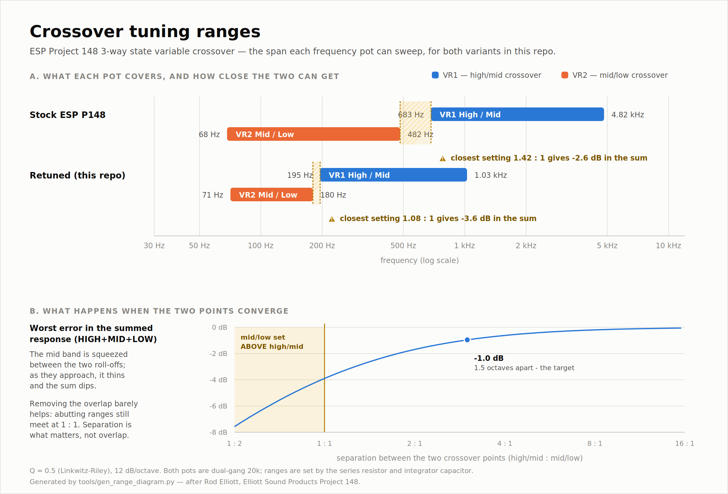
The retuned ranges don't overlap, but that is not what keeps the response flat — separation is. Because the two filters are tuned independently, nothing stops you setting them close together, and ranges that merely abut still meet at the boundary:
| Range layout | Closest possible setting | Sum error there |
|---|---|---|
| Stock ESP P148 | 1.42 : 1 | −2.62 dB |
| Retuned | 1.08 : 1 | −3.57 dB |
The outputs never swap — filter 1 is unaware of filter 2, so HIGH is
unaffected. What collapses is MID, whose passband is the gap between the two
corners: squeeze that gap and it thins out, and the summed response develops a
broad suck-out. The degradation is gradual and already measurable at 1.6 : 1,
so the rule is keep the two points at least 3 : 1 apart (~1.5 octaves) for
under 1 dB. That's setting discipline, not something the hardware enforces —
note the stock ESP values have the same exposure. Nothing is damaged or
unstable; turn VR2 back down and it recovers. Full detail in
docs/circuit-notes.md.
f = 1/(2πRC), where R sweeps from the series resistor alone to series + 20 k
pot. The series resistor therefore sets both the top frequency and the
max/min ratio:
| Variant | R7, R8 | C1, C2 | High/Mid | R17, R18 | C3, C4 | Mid/Low |
|---|---|---|---|---|---|---|
| Stock | 3.3k | 10 nF | 683 Hz – 4.82 kHz | 3.3k | 100 nF | 68.3 – 482 Hz |
| Retuned | 4.7k | 33 nF | 195 Hz – 1.03 kHz | 13k | 68 nF | 70.9 – 180 Hz |
Nothing else differs — same Q, same op-amps, same 20 k pots. Larger series resistors also load the previous stage less, so this direction is safe; the article only warns against going below ~2.2k.
Full explanation, design equations and frequency tables: docs/circuit-notes.md.
One diagram per functional block of the board, in docs/subcircuits/: input and master volume, each of the two crossover filters, the level controls, the output buffers, the two halves of the muting circuit, and power/decoupling.
They are generated, not drawn. tools/gen_schematic.py crops each block
out of the full sheet through the same render_svg() that renders the main
schematic, so the symbols, strokes and fonts are identical to it and cannot
drift. Rebuild them with:
python3 tools/gen_schematic.pyThe part-by-part tables that go with the pictures are in docs/circuit-notes.md.
The ESP figures deliberately leave out supply wiring. This schematic adds it so the netlist is complete:
The retuned-quad-smd variant — the one the board is built from — adds more
still: a master volume, per-band volume trims, buffered outputs with DC
blocking and bleeders, and per-output muting with soft start. Every part and
what it does is listed in
docs/circuit-notes.md.
These apply to the four schematic/ variants. None of them applies to the
routed board — it has real footprints, real LCSC part numbers and a
verified layout; see the next list for its limitations.
TEXT
shapes carry no pre-rendered glyph path, which is normal for generated
files and expected to work — but it is the one thing that cannot be
checked without importing.kicad/esp-p148-3way-crossover-retuned-quad-smd.kicad_sch — the same
schematic as a KiCad 8 schematic, generated by tools/gen_kicad.py.
Open kicad/crossover.kicad_pro, or the .kicad_sch on its own.
It is self-contained: every symbol is embedded in the file's own
lib_symbols, one per component instance, so nothing needs to be
installed and no library path has to resolve. Nets are carried by labels
exactly as they are drawn.
It is not a second drawing of the circuit. gen_kicad.py reads the very
geometry gen_schematic.py lays out — every pin in absolute coordinates,
every wire polyline, every label — and translates it, so the two cannot
disagree about connectivity. And it checks: after emitting the file it
parses it back, rebuilds the netlist from the geometry alone, and refuses
to write anything unless that matches the schematic's own netlist.
kicad/esp-p148-3way-crossover-retuned-quad-smd.kicad_pcb — a routing
seed, for handing to an external router or placement tool. It is placed
but not wired:
It is read from the committed pcb/*.json, so it cannot describe a board
that was never built, and the emitted file is parsed back and checked
before it is written: bare of copper, every edge part inside the outline,
every other part clear of it, pad nets identical to the board's.
pcb/esp-p148-3way-crossover-retuned-quad-smd-pcb.json — 149.6 ×
63.5 mm, four layers, fully routed, nine front-panel controls on
the board (a frequency pot and a volume trim per band, a master volume, and
a mute button per band), trace width matched to purpose (12 mil signal,
16 mil power/ground), 45° chamfered corners, every SMD part a real LCSC
line item.
The stackup is L1 signal / L2 solid GND plane / L3 signal / L4 signal.
Two layers could not route this board once the three panel mute buttons
went into the front row — see
docs/pcb-notes-smd.md.
Every part that reaches an edge is pinned into one of two rows — the panel row on the front, the connector row on the back — and nothing may sit outside either, so the board edges land 1.27 mm behind them. See Two pinned edge rows.
Every SMD ground pad is fanned out to the plane before any signal net is routed — a via on the pad, straight down. Repairing ground afterwards does not work once the traces are down, and that is what used to leave op-amp ground pins stranded.
Beyond the filter itself it carries buffered outputs with build-out
resistors, DC blocking and bleeders, a 47 kΩ line input, bulk and per-IC
supply decoupling, and per-output muting with power-up soft start — a
JFET shunting each buffer input, steering diodes so one button mutes one
band, and an RC that holds everything muted until the rails settle and
re-mutes fast when they collapse. The three mute buttons are on the
board, in the panel row beside the volume trims - right-angle push-lock
DPDTs, so their plungers come out of the board edge alongside the pot
shafts. J6 carries only the optional panel LEDs, which light when a band
is playing. No audio leaves the board. Which parts do what, block
by block, is in
docs/circuit-notes.md.
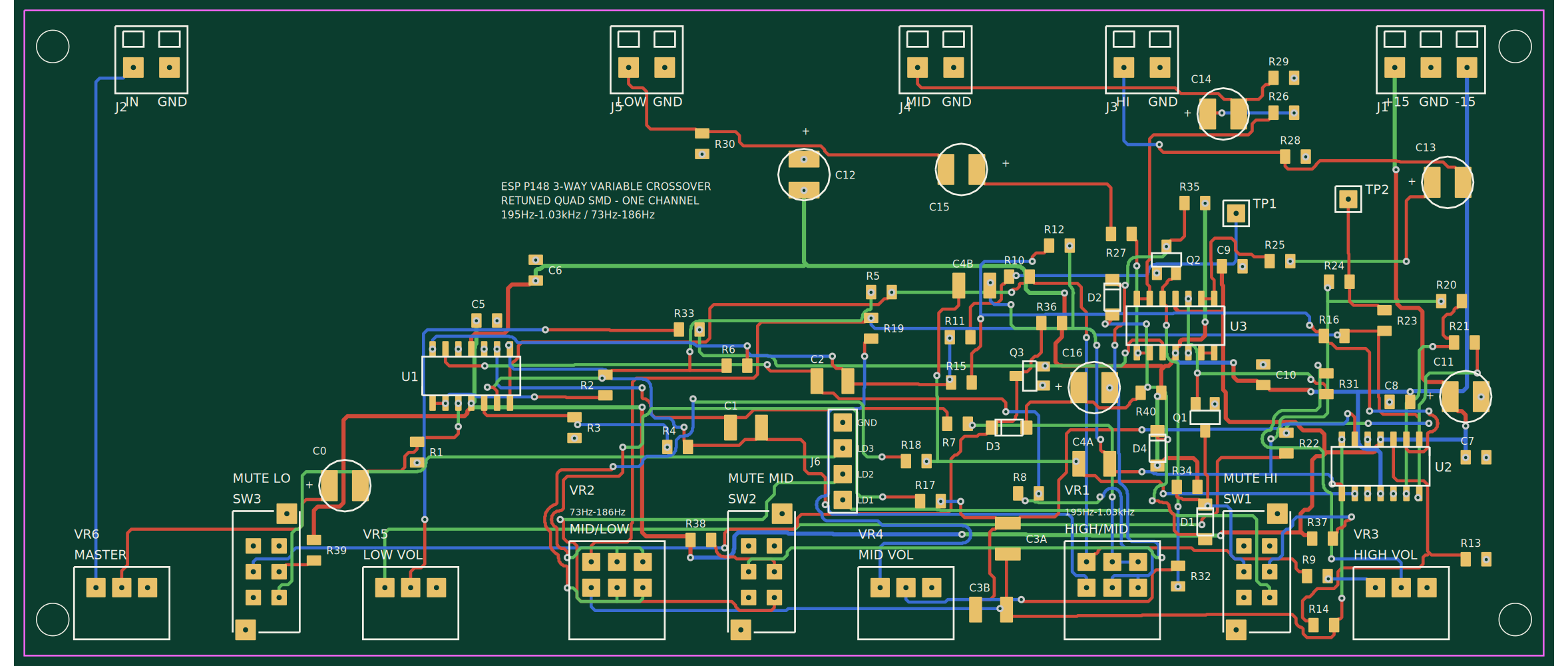
board 149.6 x 63.5 mm | 86 footprints | 242 pads | 227 tracks | 159 vias
verified: all nets connected, all clearances >= 8 mil, no unrouted nets,
          pads match the schematic exactly
On the rear edge, left to right: line input, LOW, MID, HIGH, power — the three outputs adjacent and in the same order as the front panel, with the power block at the far end from the input so the two looms never run together. On the front edge, left to right: MASTER, LOW mute, LOW volume, MID/LOW frequency, MID mute, MID volume, HIGH/MID frequency, HIGH mute, HIGH volume — nine controls, each mute button beside the volume trim it mutes. The board lies flat in the enclosure, perpendicular to the front panel, with right-angle pots and right-angle switches on the front edge and their shafts and plungers through the panel — the way a small amplifier board is usually arranged. The frequency pots carry their sweep range on the silkscreen. The volume controls are single-gang audio-taper pots (Alps RK097 pattern) wired as attenuators; the frequency pots are the standard 9 mm dual-gang pattern. Both need checking against your parts' datasheets — there are no locating-boss holes, deliberately; see the notes.
Drilling the panel: docs/panel-drilling.md
is generated from the same placement as the copper, and gives the X of every
shaft and plunger from the board's left edge, the two pitches the row uses,
and where the four mounting holes actually ended up. Regenerate the board
and that file follows it, so it cannot drift from the part positions the way
a measured-off-the-preview drawing would.
Routing is checked by geometry that doesn't reuse the router's own bookkeeping:
exact pairwise clearance between every copper feature, union-find connectivity
per net, mounting-hole keepout, footprint-courtyard overlap, and pad-set
equality with the schematic. Those checks have caught real defects that would
otherwise have reached the fab, including a pre-existing footprint overlap
between two adjacent parts that nothing before the courtyard check could even
detect — see docs/pcb-notes-smd.md.
Part numbers were looked up live against the JLCPCB parts API; re-check stock before ordering. Export Gerbers, BOM and CPL from EasyEDA rather than using the CPL in this repo — a CPL's origin has to match the Gerbers, and only EasyEDA knows that at export time.
JLCPCB won't assemble through-hole parts. 69 of the 86 footprints are machine-placed; the 17 you solder yourself are all through-hole and all of them are edge or panel hardware:
VR1–VR6 — the six potsSW1–SW3 — the three mute buttonsJ1–J5 — power in, line in, and the three outputsJ6 — the optional panel-LED headerTP1, TP2 — the two test pointsThere is no off-board pot or switch wiring any more: every control is an edge-mount part on the board itself.
The circuit is already lean, so build effort is easy to spend in the wrong place. In order of what actually measures:
retuned-quad
variant. The circuit splits perfectly at the filter boundary, four sections
each, so one quad per filter: half the ICs, half the bypass caps, smaller
board, no circuit change. Drawn with the MC33079 (closest in character to
the NE5532); any standard quad pinout drops in — OPA1644, OPA4134,
LME49740, TL074.Things that look like simplifications but aren't: the input buffer U1A keeps
source impedance out of the Q and gain; the integrators have no DC feedback of
their own, so the state-variable loop must stay intact. Detail in
docs/circuit-notes.md.
Circuit design © Rod Elliott, Elliott Sound Products, Project 148 (2014). The ESP article grants personal use and one printed copy for reference while building; commercial use needs Rod Elliott's written permission. This repository holds a re-drawn schematic for personal construction — please read the article itself, and buy the ESP PCB if you want one.
| Qty | Value | Footprint | References |
|---|---|---|---|
| 10 | 5.6k | crossover:0805 | R2, R4, R5, R6, R12, R14, R15, R16, R20, R21 |
| 7 | 10k | crossover:0805 | R10, R11, R23, R24, R31, R32, R33 |
| 7 | 10uF | crossover:CASE-D5xL5.4 | C0, C11, C12, C13, C14, C15, C16 |
| 6 | 100R | crossover:0805 | R9, R19, R22, R25, R26, R27 |
| 6 | 100nF | crossover:0805 | C5, C6, C7, C8, C9, C10 |
| 6 | 33nF | crossover:1210 | C1, C2, C3A, C3B, C4A, C4B |
| 4 | 1M | crossover:0805 | R34, R35, R36, R40 |
| 4 | 1N4148W | crossover:SOD-123 | D1, D2, D3, D4 |
| 4 | TB-2P-3.5 | crossover:TB-2P-3.5 | J2, J3, J4, J5 |
| 4 | — | crossover:MountingHole | H1, H2, H3, H4 |
| 3 | 100k | crossover:0805 | R28, R29, R30 |
| 3 | 10k log | crossover:POT-9MM-SINGLE | VR3, VR4, VR5 |
| 3 | 2.2k | crossover:0805 | R37, R38, R39 |
| 3 | DPDT LOCK | crossover:SW-PS22E05 | SW1, SW2, SW3 |
| 3 | MC33079 | crossover:SOIC-14 | U1, U2, U3 |
| 3 | MMBFJ112 | crossover:SOT-23 | Q1, Q2, Q3 |
| 2 | 11k | crossover:0805 | R3, R13 |
| 2 | 13k | crossover:0805 | R17, R18 |
| 2 | 20k dual | crossover:POT-9MM-DUAL | VR1, VR2 |
| 2 | 4.7k | crossover:0805 | R7, R8 |
| 1 | 47k | crossover:0805 | R1 |
| 1 | 50k log | crossover:POT-9MM-SINGLE | VR6 |
| 1 | MUTE | crossover:HDR-1X4 | J6 |
| 1 | TB-3P-3.5 | crossover:TB-3P-3.5 | J1 |
| 1 | TP1 | crossover:THT-PAD | TP1 |
| 1 | TP2 | crossover:THT-PAD | TP2 |
It measures 149.6 × 63.5 mm and has 4 copper layers, 1.6 mm thick.
90 parts, built around the MC33079D, 1N4148W, MMBFJ112 and TP1. The full list of its parts is on this page, with links to each part's symbol and footprint where PCBKit's library has them.
From the nict41/crossover repository on GitHub, at the commit this page was made from: the board is kicad/esp-p148-3way-crossover-retuned-quad-smd.kicad_pcb and its schematic kicad/esp-p148-3way-crossover-retuned-quad-smd.kicad_sch. PCBKit opens the board in the browser, with nothing to install.
Its repository states no licence, so its author keeps all rights: ask nict41 before reusing the design.


Orthogonal-Systems/MegaDAQ
Data acquisition shield for VMEMega system compatible with arduino mega boards. 16 12b ADCs and 12 12b DACs.


