2 layers171.7 × 97.4 mm
Hhkb split right
ms0216/hhkb-split
HHKB Professional HYBRID Type-S の使い勝手を再現する完全分割型キーボード(ZMK / XIAO nRF52840 / build123d による寸法駆動CAD)
83 parts1
 ms0216/hhkb-split1
HHKB Professional HYBRID Type-S の使い勝手を再現する完全分割型キーボード(ZMK / XIAO nRF52840 / build123d による寸法駆動CAD)
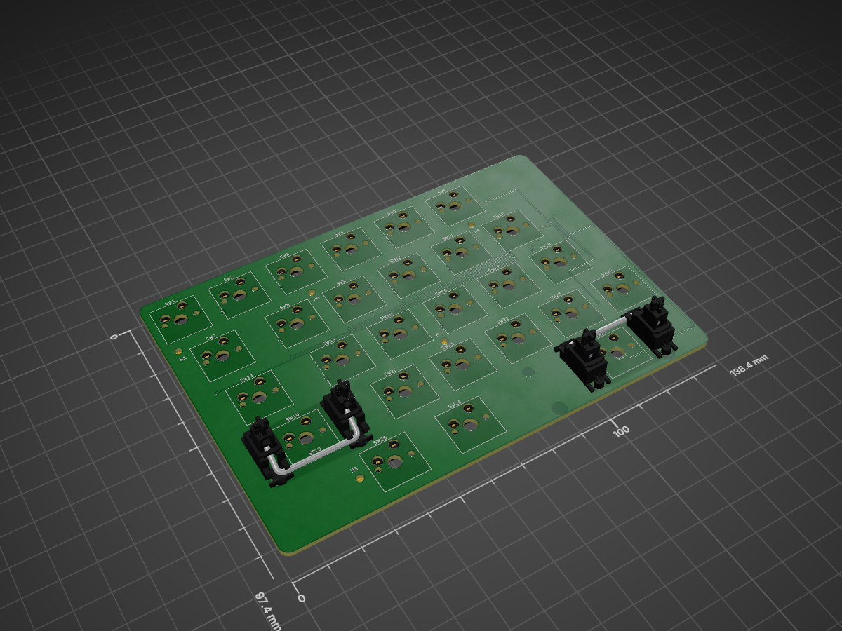
Hhkb split left is an open-source printed circuit board by ms0216, from the ms0216/hhkb-split repository on GitHub. It is a 2-layer board of 138.4 × 97.4 mm with 65 parts on 45 nets, routed with 291 tracks and 66 vias.
It is built around the 74LVC595AD, BAT46W and CPG151101S11-2, with the FH12-12S-0.5SH(55) among its other parts. Its parts include 27 diodes, 27 switches and 1 IC.


| 段階 | 内容 | 状態 |
|---|---|---|
| D1 | 外形・キー配置・取付穴 | ✅ 完了。DRC 違反 0 |
| D2a | マトリクス(61キー + 61ダイオード + 行列のネット) | ✅ 完了 |
| D3a | マトリクスの配線(行・列・スイッチ→ダイオード) | ✅ 左は違反 0 / ⚠️ 右に 5 件(下記) |
| D2b | XIAO・74HC595・電源の搭載 | ⬜ 3D 実装の検討が要る(下記) |
| D3 | 配線(行・列・電源) | ⬜ |
| D4 | JLCPCB 向け出力(ガーバー・BOM・CPL) | ⬜ |
マトリクスは配線済み(未配線 0)。左半分は DRC 違反 0。
すべて hole_clearance(配線が穴に近すぎる)で、原因は特定済み。
列のバスは行間の空きを横に渡るが、スタビライザーの穴がその帯に食い込んで いる(キー中心 +6.2〜10.2mm)。9 列ぶんの通り道を 0.8mm 間隔で並べると、 穴を避けきれない列が出る。
取りうる手:
左半分が完全に通っているので、方式の問題ではない。
XIAO は基板の裏面に付く(表に置くとキーキャップと当たる)。ところが USB-C は実機と同じく背面に出す必要があり、基板の裏の背面側には **電池室(幅 109mm)**が横断している。左半分では電池の外側に 15mm ほどしか残らず、XIAO の 17.8mm が入らない。
取りうる案:
ケースの 3D モデルと合わせて検討する必要がある。 実測(Task C4)で 電源部の構成が確定してから着手するのが順序として正しい。
pcbnew は KiCad 同梱の Python にしか無いので、そちらで動かす。
/Applications/KiCad/KiCad.app/Contents/Frameworks/Python.framework/Versions/3.9/bin/python3.9 \
tools/gen_pcb.py# デザインルール検査(違反があれば終了コードが非 0)
/Applications/KiCad/KiCad.app/Contents/MacOS/kicad-cli pcb drc \
--severity-error --exit-code-violations pcb/hhkb_split_left.kicad_pcb
# 生成物が設計値と一致するか(通常の pytest から実行できる)
python -m pytest tools/test_pcb.py
# 目で見る
/Applications/KiCad/KiCad.app/Contents/MacOS/kicad-cli pcb render \
--output /tmp/pcb.png --side top pcb/hhkb_split_left.kicad_pcb.kicad_pcb はテキスト(S 式)なので、tools/test_pcb.py は pcbnew 無しで
読める。生成した基板を読み返して、プレート・ケースと突き合わせるのが要点。
別々に生成される以上、同じ設計値から導いていても座標変換を間違えれば静かに
ずれる。ずれたまま発注すると数万円が無駄になる。
| 左 | 右 | |
|---|---|---|
| 基板 | 140.36 × 102.00mm | 173.70 × 102.00mm |
| スイッチ | 27 | 34 |
| スタビライザー | 2 | 2 |
| 取付穴 | 7 | 7 |
外形はプレートより片側 3.0mm 小さい(interface.PCB_INSET)。ケースの
側壁 2.4mm の内側に収める必要があるため。
奥行 102.00mm = プレート 108.00mm − 6.0mm。プレートの 108.00mm は HHKB 実機の本体奥行そのもの。
lib/ を参照。KiCad 標準に無い 3.00u とホットスワップソケットだけを
kiswitch から取り込み、寸法を規格値と照合してある。
| Qty | Value | Footprint | References |
|---|---|---|---|
| 27 | BAT46W | D_SOD-123 | D1, D2, D10, D11, D12, D13, D14, D15, D16, D17, D18, D19, D20, D21, D22, D23 +11 |
| 22 | CPG151101S11-2 | SW_Hotswap_Kailh_MX_1.00u | SW1, SW2, SW10, SW11, SW12, SW14, SW15, SW16, SW17, SW18, SW20, SW21, SW22, SW23, SW24, SW25 +6 |
| 6 | MountingHole_2.2mm_M2 | MountingHole_2.2mm_M2 | H0, H1, H2, H3, H4, H5 |
| 2 | CPG151101S11-2 | SW_Hotswap_Kailh_MX_1.50u | SW7, SW26 |
| 2 | Stabilizer_Cherry_MX_2.00u | Stabilizer_Cherry_MX_2.00u | ST19, ST27 |
| 1 | 100nF | C_0805_2012Metric | C_U1 |
| 1 | 74LVC595 | TSSOP-16_4.4x5mm_P0.65mm | U1 |
| 1 | CPG151101S11-2 | SW_Hotswap_Kailh_MX_2.25u | SW19 |
| 1 | CPG151101S11-2 | SW_Hotswap_Kailh_MX_1.75u | SW13 |
| 1 | CPG151101S11-2 | SW_Hotswap_Kailh_MX_2.75u | SW27 |
| 1 | FH12-12S-0.5SH(55) | Hirose_FH12-12S-0.5SH_1x12-1MP_P0.50mm_Horizontal | J_DB |
It measures 138.4 × 97.4 mm and has 2 copper layers, 1.6 mm thick.
65 parts, built around the 74LVC595AD, BAT46W, CPG151101S11-2 and FH12-12S-0.5SH(55). The full list of its parts is on this page, with links to each part's symbol and footprint where PCBKit's library has them.
From the ms0216/hhkb-split repository on GitHub, at the commit this page was made from: the board is pcb/matrix_only/hhkb_split_left.kicad_pcb and its schematic pcb/hhkb_split_daughterboard.kicad_sch. PCBKit opens the board in the browser, with nothing to install.
Its repository states no licence, so its author keeps all rights: ask ms0216 before reusing the design.
ms0216/hhkb-split
HHKB Professional HYBRID Type-S の使い勝手を再現する完全分割型キーボード(ZMK / XIAO nRF52840 / build123d による寸法駆動CAD)

ms0216/hhkb-split
HHKB Professional HYBRID Type-S の使い勝手を再現する完全分割型キーボード(ZMK / XIAO nRF52840 / build123d による寸法駆動CAD)

vyquocvu/analog-ai-chip
This directory contains the editable KiCad 10 source for the 70 mm × 52 mm, four-layer Pager-1 main carrier. The display, keypad, protected Li-Po pack, and analog accelerator are external assemblies.

6thSense-dev/mocap-glove
Magnetic MoCap glove firmware, tracking diagnostics and local hand visualizer

MLeggiero/taxelscan
TaxelScan reads a 16 × 32 pressure surface (512 taxels) at 80 frames per second by default and has been measured at 200 fps.

roberto314/Unicomp2
A modular 8-bit Computer able to recreate (nearly) every Retro computer of the late 70s to mid 80s.


roberto314/Unicomp3
A modular 8-bit Computer able to recreate (nearly) every Retro computer of the late 70s to mid 80s.

