Skip to the content
PCBKitNew board
2 layers78.4 × 68 mmHcppnfc, the printed circuit board in 3D

The Sekura Monero Hardware Wallet

Size
78.4 × 68 mm
Copper layers
2
Thickness
1.6 mm
Parts
13
Nets
17
Pads
30
Tracks, vias
28, 2
Pours
2
Routed
Yes
KiCad
KiCad 4
Created
18 Oct 2017
Updated
28 Jan 2020

Overview

Hcppnfc is an open-source printed circuit board by monero-project, from the monero-project/kastelo repository on GitHub. It is a 2-layer board of 78.4 × 68 mm with 13 parts on 17 nets, routed with 28 tracks and 2 vias.

It is built around the M24SR02-YMN6T/2. Its parts include 2 ICs and 2 switches.

Main components

1

README

hardware/breakneck/README.md

Hardware Breakneck Design

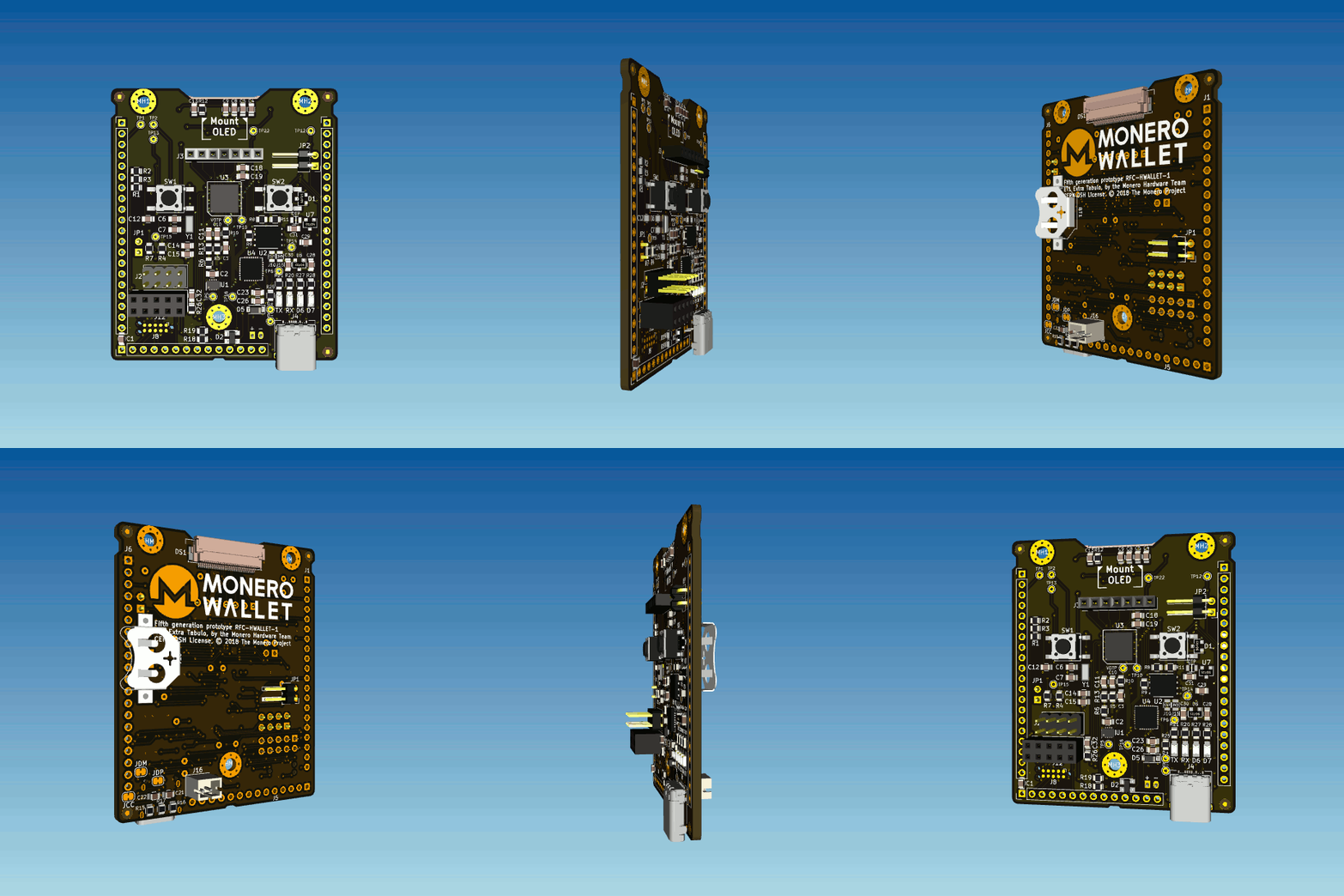
The Breakneck design includes rich features typical of a developer edition hardware wallet.

Breakneck schematic print

Breakneck CAD layout  Breakneck board layout  Breakneck shaded animation

Getting Started

The Breakneck design consists of several files, some which are not tracked in revision control but are part of project releases.

  • breakneck.pro (KiCad project)
  • breakneck.sch (KiCad schematic)
  • breakneck.kicad_pcb (KiCad layout)
  • libraries (KiCad libraries)
  • modules (KiCad footprints)

Fabrication subdirectories contain files meant for printing, assembly, and other production work.

  • billofmat (Bill of materials generated from the layout)
  • fabpanel (Gerber files for printing panelized PCBs)
  • fabraster (3D rendition of a single PCB layout)
  • fabsingle (Gerber files for printing single PCBs)
  • fabvector (Vector files useful for mechanical engineering)

Other subdirectories exist to provide conveniently formatted files generated from source.

  • release (Tested distribution release files containing change logs)
  • schematic (Copy of breakneck.sch converted to common graphic formats)

A Makefile serves project management tasks allowing for scripting and automation.

  • Makefile (A GNU Makefile facilitating command line project tasks)

Parts

13
QtyValueFootprintReferences
3Dummy_FIDUCIAL_Passermarke_Type1_RevE_Date16Nov2011Monero_HW:Fiducial_1mm_Dia_2mm_OuterFID1, FID2, FID3
2M24SR02-YMNMonero_HW:SOIC-8_3.9x4.9mm_Pitch1.27mmU1, U2
1ART_CONFYEARMonero_HW:HCPPNewordconfGFX*
1ART_INSTCRYPMonero_HW:HCPPNewordinstGFX*
1ART_TRIANGLEMonero_HW:HCPPNewordtriGFX*
1Antenna_LoopMonero_HW:NFCAntennatallAE1
1DUMMY_MOUNTING-HOLE_RevE_Date22jun2010Monero_HW:MountingHole_4.3mm_M4_ISO14580_PadMH1
1LOGOMonero_HW:HCPPSponsorsLOGO*
1SW_SPSTMonero_HW:SW_SPST_K21102SPSW1
1SW_SPSTMonero_HW:SW_SPST_PTS645SW2

Questions

How big is the Hcppnfc PCB?

It measures 78.4 × 68 mm and has 2 copper layers, 1.6 mm thick.

What parts does the Hcppnfc use?

13 parts, built around the M24SR02-YMN6T/2. The full list of its parts is on this page, with links to each part's symbol and footprint where PCBKit's library has them.

Where can I download the Hcppnfc KiCad files?

From the monero-project/kastelo repository on GitHub, at the commit this page was made from: the board is hardware/confbadge/hcppnfc/hcppnfc.kicad_pcb. PCBKit opens the board in the browser, with nothing to install.

Can I use the Hcppnfc design in my own project?

Its repository states no licence, so its author keeps all rights: ask monero-project before reusing the design.

More from monero-project/kastelo

7
  • 2 layers145 × 165 mmBreakpanel, the printed circuit board in 3D

    Breakpanel

    monero-project/kastelo

    The Sekura Monero Hardware Wallet

    690 parts115
  • 2 layers53.3 × 64 mmBreakneck, the printed circuit board in 3D

    Breakneck

    monero-project/kastelo

    The Sekura Monero Hardware Wallet

    124 parts115
  • 2 layers100 × 95 mm35C3XMR, the printed circuit board in 3D

    35C3XMR

    monero-project/kastelo

    The Sekura Monero Hardware Wallet

    97 parts115
  • 2 layers60.5 × 45.8 mmLedgblue, the printed circuit board in 3D

    Ledgblue

    monero-project/kastelo

    The Sekura Monero Hardware Wallet

    61 parts115
  • 2 layers70 × 100 mmDefconfc, the printed circuit board in 3D

    Defconfc

    monero-project/kastelo

    The Sekura Monero Hardware Wallet

    39 parts115
  • 2 layers53.3 × 64 mmBreaknext, the printed circuit board in 3D

    Breaknext

    monero-project/kastelo

    The Sekura Monero Hardware Wallet

    15 parts115
  • 2 layers66 × 21 mmUsbconntest, the printed circuit board in 3D

    Usbconntest

    monero-project/kastelo

    The Sekura Monero Hardware Wallet

    6 parts115

Similar boards

  • 2 layers122.5 × 115.6 mmInitialDesign, the printed circuit board in 3D

    InitialDesign

    ozseccon/ozseccon-dev-badge

    OzSecCon Badge Dev environment

    49 parts1
  • 2 layers40 × 20 mmUsb uart, the printed circuit board in 3D

    Usb uart

    earthtojake/text-to-cad

    Design physical products with AI

    13 parts26kMIT
  • 2 layers35 × 29 mmMagSpoofTC, the printed circuit board in 3D

    MagSpoofTC

    samyk/magspoof

    A portable device that can spoof/emulate any magnetic stripe, credit card or hotel card "wirelessly", even on standard magstripe (non-NFC/RFID) readers.

    13 parts4.2k
  • 2 layers20.6 × 23.6 mmAO-03 signal amplifier, the printed circuit board in 3D

    AO-03 signal amplifier

    fossasia/pslab-scripts

    Pocket Science Lab - Scripts for Sensor Experiments

    13 parts1.6kApache-2.0
  • 2 layers47 × 35.6 mmMX7-C-35PL C11, the printed circuit board in 3D

    MX7-C-35PL C11

    rusefi/rusefi

    rusefi - GPL internal combustion engine control unit

    13 parts1.2k
  • 2 layers95 × 95 mmCube batteryboard, the printed circuit board in 3D

    Cube batteryboard

    willem-pennings/balancing-cube

    A cube that balances itself in a corner or edge using reaction wheels

    13 parts1.1kGPL-3.0
  • 2 layers15.2 × 20.3 mmPt100stick, the printed circuit board in 3D

    Pt100stick

    VoronDesign/Voron-Hardware

    Cool Hardware designed by the Voron Design group

    13 parts1.1kGPL-3.0