2 layers55 × 100 mm

 MohamedAlDeep/EEG-Headset1
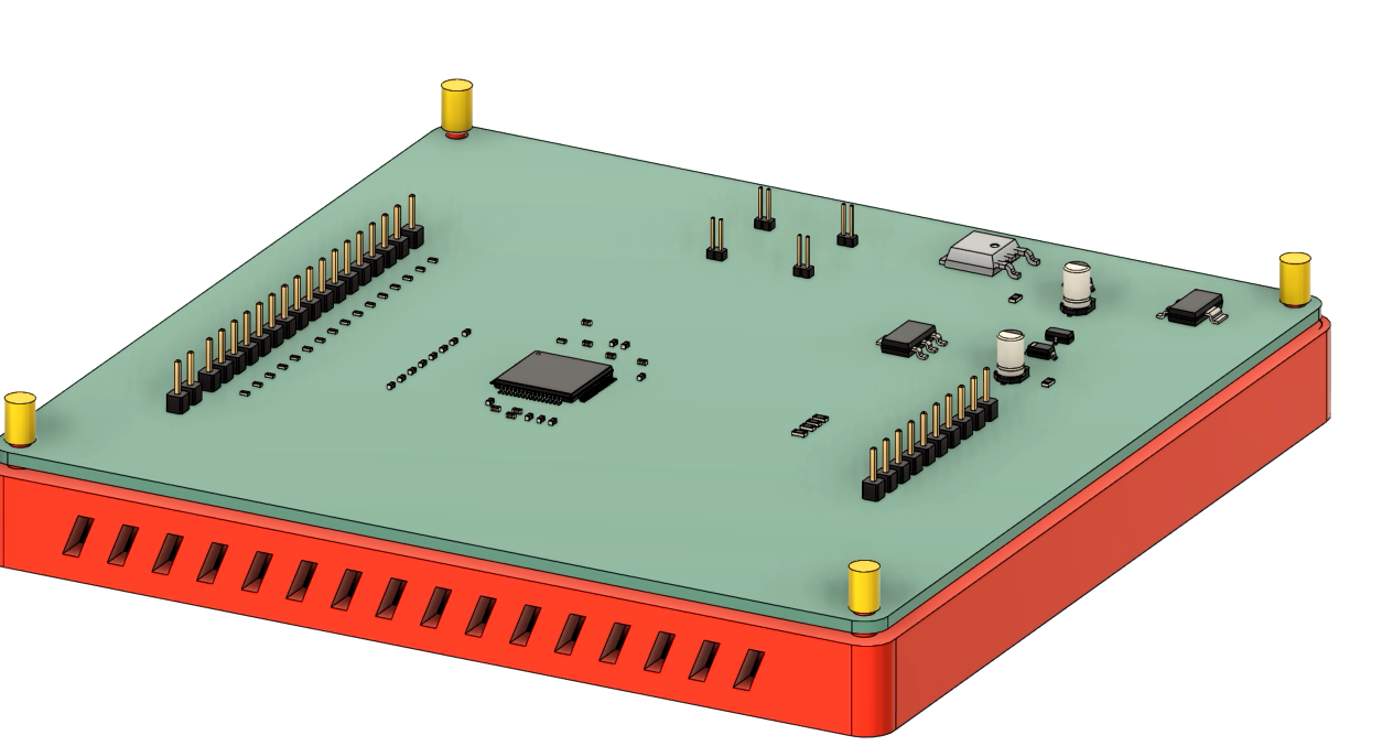
This is the main board for EEG reading headset, in which it uses an analogue to digital converted (ADS1299) chip. Such devices made by companies are expensive, the goal is to make it using the same components but DIY.
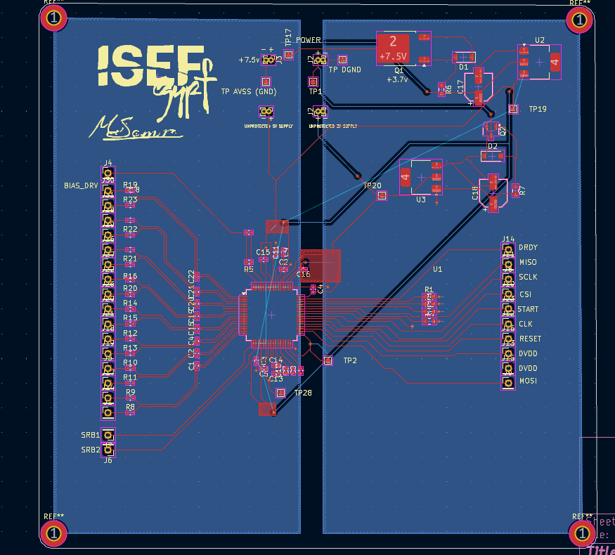
PCB Design is an open-source printed circuit board by MohamedAlDeep, from the MohamedAlDeep/EEG-Headset repository on GitHub. It is a 2-layer board of 113 × 110.5 mm with 100 parts on 55 nets, routed with 589 tracks and 21 vias.
It is built around the AMS1117-3.3 and IRLML6402. Its parts include 33 connectors, 24 capacitors, 23 resistors, 3 ICs and 2 diodes.


This is a DIY / custom electroencephalogram reading device which is connected eeg electrodes that can connect to brain at designated areas.
It reads brain wave signals and digitizes them into the computer which is called brain-computer interface.
I have a larger project and i want to join the competition with my pcb.
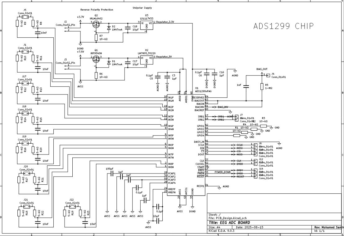
This is the board schematic.
| Qty | Value | Footprint | References |
|---|---|---|---|
| 29 | Conn_01x01 | Connector_PinHeader_2.00mm:PinHeader_1x01_P2.00mm_Vertical | J1, J10, J11, J12, J13, J14, J15, J16, J17, J18, J19, J20, J21, J22, J23, J24 +13 |
| 16 | 5-kΩ | Resistor_SMD:R_0402_1005Metric | R8, R9, R10, R11, R12, R13, R14, R15, R16, R17, R18, R19, R20, R21, R22, R23 |
| 9 | 10nF | Capacitor_SMD:C_0402_1005Metric | C1, C2, C4, C12, C15, C19, C20, C21, C22 |
| 8 | TestPoint | TestPoint:TestPoint_Pad_1.0x1.0mm | TP AVSS (GND), TP DGND, TP1, TP2, TP17, TP19, TP20, TP28 |
| 7 | 1μF | Capacitor_SMD:C_0402_1005Metric | C2, C3, C8, C9, C10, C15, C16 |
| 6 | 10-kΩ | Resistor_SMD:R_0603_1608Metric | R1, R2, R3, R4, R6, R7 |
| 4 | Conn_01x02_Pin | Connector_PinHeader_1.00mm:PinHeader_1x02_P1.00mm_Vertical | J2, J2, J3, UNPROTECTED 5V SUPPLY |
| 3 | 0.1μF | Capacitor_SMD:C_0402_1005Metric | C5, C11, C13 |
| 2 | 10μF | Capacitor_SMD:CP_Elec_5x5.4 | C17, C18 |
| 1 | 1-MΩ | Resistor_SMD:R_0402_1005Metric | R5 |
| 1 | 100nF | Capacitor_SMD:C_0402_1005Metric | C4 |
| 1 | 100μF | Capacitor_SMD:C_0402_1005Metric | C7 |
| 1 | 10μF | Capacitor_SMD:C_0402_1005Metric | C14 |
| 1 | 1N47xxA | Diode_SMD:D_SOD-123 | D2 |
| 1 | ADS1299xPAG | Package_QFP:TQFP-64_10x10mm_P0.5mm | U1 |
| 1 | AMS1117-3.3 | Package_TO_SOT_SMD:SOT-223 | U3 |
| 1 | BZT52C5V1-W8 5.1V Zener 500mW | Diode_SMD:D_SOD-123 | D1 |
| 1 | FQD4P50 (P-MOSFET) | Package_TO_SOT_SMD:TO-252-2 | Q1 |
| 1 | IRLML6402 | Package_TO_SOT_SMD:SOT-23 | Q2 |
| 1 | LM7805_TO220 | Package_TO_SOT_SMD:SOT-223 | U2 |
| 1 | LOGO | Logo:LogoSignedFoot | G*** |
The 96 most common of 100 parts.
It measures 113 × 110.5 mm and has 2 copper layers, 1.6 mm thick.
100 parts, built around the AMS1117-3.3 and IRLML6402. The full list of its parts is on this page, with links to each part's symbol and footprint where PCBKit's library has them.
From the MohamedAlDeep/EEG-Headset repository on GitHub, at the commit this page was made from: the board is PCB/PCB_Design.kicad_pcb and its schematic PCB/PCB_Design.kicad_sch. PCBKit opens the board in the browser, with nothing to install.
Its repository states no licence, so its author keeps all rights: ask MohamedAlDeep before reusing the design.


DerSchweigefuchs/uC_Agri-PV
A custom PCB designed for environmental monitoring in agricultural photovoltaic installations. Built around the STM32U5 ultra-low-power microcontroller with LoRaWAN connectivity and multiple sensor interfaces.


paagutie/bluerov_acmodule
DIY Board developed as actuator module using micro-ROS as middelware.

lachlanA/eagle-to-kicad
Eagle SCH/LIB to KiCad SCH/LIB ULP conversion script