DEV_Board_By_Mo3 (ESP8266-12E)
A custom-designed, high-performance development board based on the ESP-12E (ESP8266) module. This board features a modern USB-C interface and is designed for seamless prototyping with integrated power regulation and USB-to-TTL conversion.
🚀 Key Features
- Core Microcontroller: ESP8266-12E module with integrated PCB antenna.
- Modern Interface: USB-C 16-pin receptacle for power and programming.
- Stable Power: AMS1117-3.3V LDO regulator providing consistent 3.3V power from the 5V USB input.
- USB-to-Serial: Integrated CH340C bridge chip for plug-and-play serial communication.
- Protection: Includes a BZW55B3V3 Zener diode and decoupling capacitors for voltage stability and ESD protection.
- Manual Controls: Dedicated Flash (DTR/RTS logic) and Reset (SW_SPST) buttons for easy bootloader access.
🛠 Hardware Architecture
The board is logically divided into four main sections as defined in the schematics:
| Section | Components | Purpose |
|---|
| Source | AMS1117-3.3, BZW55B3V3, C1, C3 | Voltage regulation and power filtering. |
| USB | USB-C 16P, D2 Diode, C6 | Power input and basic surge protection. |
| USB to TTL | CH340C, C4, C5, R4, R5 | Bridge between PC USB and ESP8266 UART. |
| ESP8266 | ESP-12E, Reset/Flash Switch, I/O Headers | Main processing, GPIO breakout, and boot mode selection. |
📐 Pinout & Connectivity
The board breaks out all essential GPIOs via two main headers:
- Header J3: GPIO12, GPIO13, GPIO14, GPIO15, GPIO16, and GND.
- Header J4: RESET, SCK, MOSI, MISO, and GND.
- Header J5: ADC and various ID pins for expanded peripheral support.
🖥️ Setup and Programming
- Driver Installation: Ensure the CH340 drivers are installed on your computer.
- Arduino IDE Configuration: * Add the ESP8266 board URL to your preferences.
- Select "NodeMCU 1.0 (ESP-12E Module)" or "Generic ESP8266 Module".
- Flashing: Use the USB-C cable to connect to your PC. The board features an auto-reset circuit (DTR/RTS) for automatic flashing, but manual buttons are available if needed.
🖼️ Gallery
2D Layout & Routing
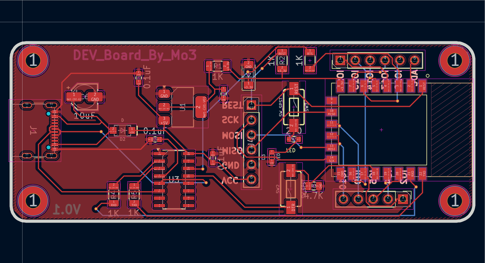
Double-layer design with optimized ground pours for RF stability.
3D Render
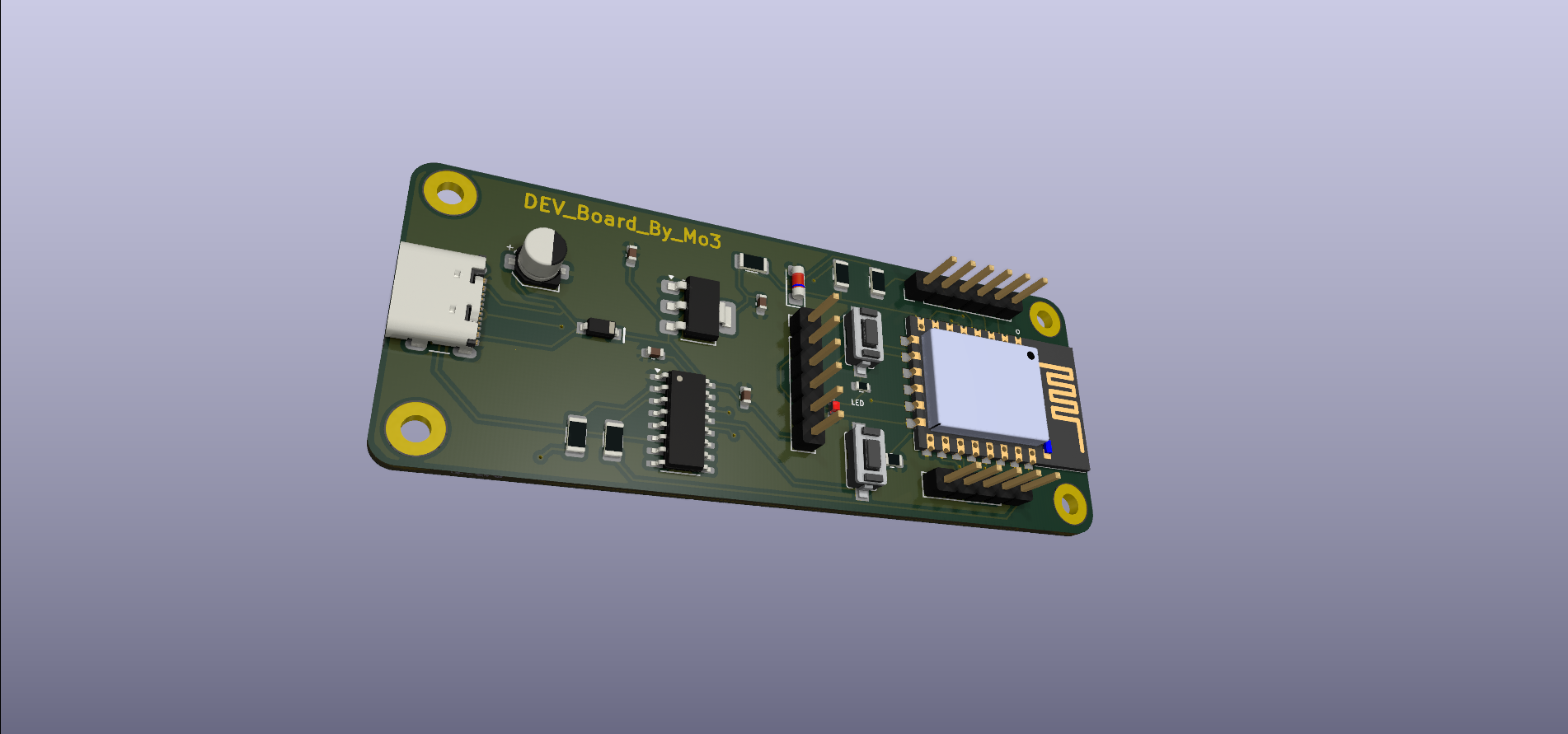
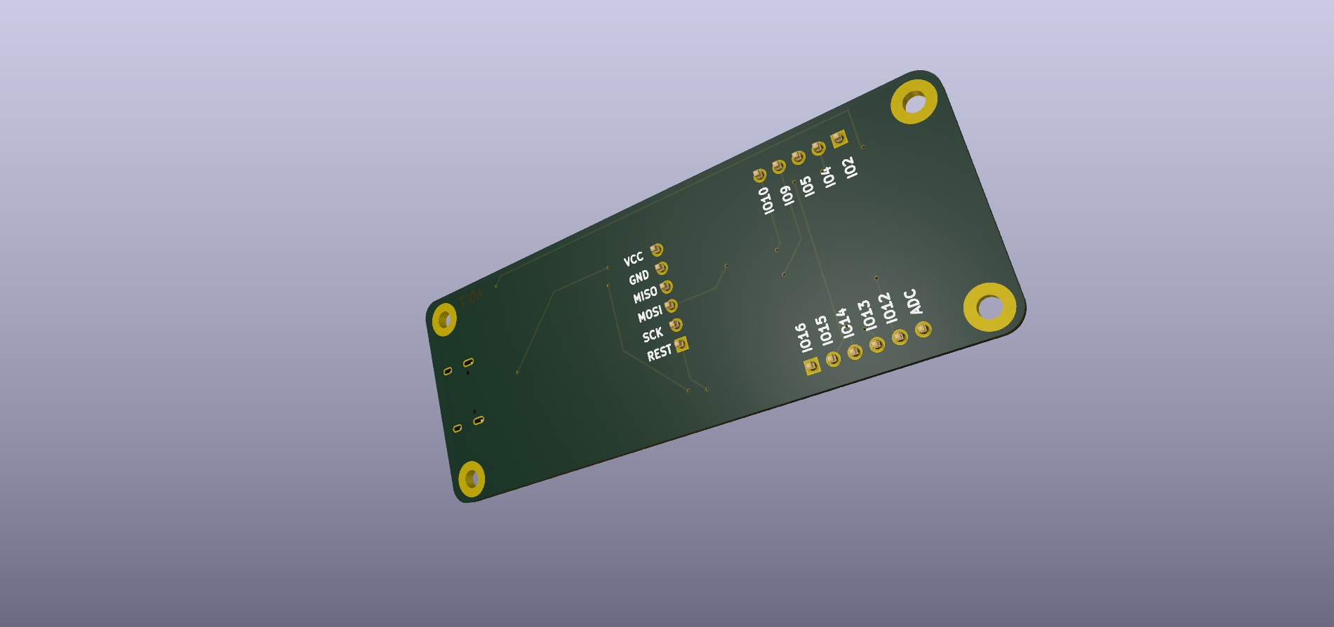 Fully assembled view showing component placement and compact form factor.
📜 License
This project is open-source. Feel free to use, modify, and distribute it for your own IoT applications.