2 layers102.4 × 211.3 mm
Haxophone001
cardonabits/haxo-hw
Haxophone, an electronic musical instrument that resembles a saxophone
92 parts674

 mniedermaier/CybICS77
Understanding industrial Cybersecurity.
CybICS is an open-source printed circuit board by mniedermaier, from the mniedermaier/CybICS repository on GitHub, published under the MIT licence. It is a 2-layer board of 160 × 100 mm with 92 parts on 124 nets, routed with 604 tracks and 96 vias.
Its parts include 52 resistors, 19 diodes, 4 capacitors, 4 connectors and 3 switches. It belongs with the STM32 boards of this library.
This guide provides detailed instructions for ordering the CybICS PCB from JLCPCB with full assembly service. The PCB is designed to be manufactured and assembled by JLCPCB, eliminating the need for manual soldering.
The PCB is designed using KiCad 10.x and all source files are available in this directory. The sources are stored in the KiCad 10 file format, so KiCad 8 and 9 cannot open them -- install KiCad 10 or later before doing anything below:
cybics.3dshapes/ holds the models KiCad does not ship. Each one that was
generated rather than downloaded keeps its build script next to it, so it can
be regenerated instead of being an unmaintainable binary:
| Model | Source | Notes |
|---|---|---|
Raspberry_Pi_Zero.step | Raspberry_Pi_Zero.build.py (CadQuery) | J1's second model, so the Pi appears plugged onto the board |
LCD1602.step | LCD1602.build.py (CadQuery) | DS1; replaces KiCad's WC1602A.step |
SW-SMD_8P-...step/.wrl | vendor download (LCSC C2858287) | navigation switch SW3 |
USB_C_Receptacle_G-Switch_GT-USB-7010ASV.wrl | easyeda2kicad --lcsc_id=C2988369 | J4; KiCad ships no model for this footprint |
The Pi Zero model sits 11.0 mm above the board: 2.5 mm for the male header body
on the carrier plus 8.5 mm for the socket on the Pi's underside, which is the
standard Pi HAT spacing. The Pi is mounted component side up -- despite
"FaceDown" in the footprint name -- so the model puts every part on the top
face. Check doc/pics/cybics.png if in doubt; that photograph is what the
model was built against.
Outline, mounting holes and the three edge-connector centres come from the official mechanical drawing; component positions are measured off that photograph and agree with the drawing's connector centres to about 0.4 mm, which is what fixes the scale. The parts are simplified shapes rather than vendor geometry, but carry the detail that makes a render readable: silkscreen frame and lettering, plated rings around the mounting holes, the raspberry on the SiP, a stamped microSD lid, recessed connector mouths, gold test pads, and passives split into black chip resistors and pale MLCCs the way the photograph shows them.
The female 2x20 socket on the Pi's underside is modelled, with a hole at each pin position so it mates with the board's male header instead of intersecting it. It is drawn 0.05 mm short on purpose: the stock header model's body measures 2.53 mm rather than the nominal 2.50, which would otherwise leave a sliver of overlap across the whole connector and make every clash check report it.
Two caveats. The PCB thickness of 1.4 mm is an assumption, as the drawing does
not state one. And the microSD card protrudes 2.1 mm past the board edge, which
is outside J1's F.Fab envelope -- that is real, not an error, and worth
knowing when designing an enclosure.
KiCad's Display.3dshapes/WC1602A.step is one fused solid, so the whole module
takes a single colour: pale green board, grey frame, blank white screen. The
replacement splits it into parts and colours them from the photograph -- dark
green board, black bezel, vivid blue screen -- and draws the characters as a
real 5 x 8 dot matrix, because a smooth outline font does not read as an LCD.
The screen shows CybICS and nothing more: the firmware also prints a version
and an uptime there, but both would go stale in a file nobody thinks to
regenerate.
Its envelope was recovered by slicing the stock model in Z and matches it exactly (80 x 36 x 15 mm), so it drops in at the same place.
Regenerate either model with:
cd hardware/pcb/cybics.3dshapes
python3 -m venv .venv && .venv/bin/pip install cadquery
.venv/bin/python Raspberry_Pi_Zero.build.py
.venv/bin/python LCD1602.build.py
J4 used to render as nothing at all. The board pointed at
${KICAD10_3DMODEL_DIR}/Connector_USB.3dshapes/USB_C_Receptacle_G-Switch_GT-USB-7010ASV.step,
which is exactly what the KiCad 10 library footprint declares -- but that file
does not exist. Not locally, and not upstream: Connector_USB.3dshapes holds 13
models in total and none of them is a G-Switch part, so 62 of the library's 75
USB footprints have no model. An earlier note here blamed the Ubuntu package;
that was wrong, kicad-packages3d 10.0.6 is complete at 3.2 GB and 7251 STEP
files. Installing more would never have fixed it.
The model now comes from the vendor via easyeda2kicad, the same route the
navigation switch took, and lives in cybics.3dshapes/.
Vendor models do not share KiCad's footprint origin. The EasyEDA footprint
for this part sits 1.325 mm in +Y from the KiCad library one, so the model
carries (offset (xyz 0 1.325 0)) -- note that the offset's Y is negated
relative to the footprint's Y. The way to check an offset is not to reason about
the sign but to compare extents: with this offset the model spans
x -4.470..4.470 and y -3.675..4.225, against the footprint's F.Fab at
x -4.470..4.470 and y -3.675..3.675. X matches exactly and so does the front
edge; the 0.55 mm at the back is the shield tab, which F.Fab does not draw.
A model's .step and .wrl need not share an origin either. SW3's do
not: the STEP has its origin at the top of the switch body, the VRML at the
board surface. A Z offset measured on one and applied to the other put the
switch 1.85 mm in the air in every render. The board references the .wrl, so
measure that one.
KiCad (version 10.0 or later)
sudo add-apt-repository ppa:kicad/kicad-10.0-releases && sudo apt install kicadFabrication Toolkit Plugin (for KiCad)
.kicad_pro)
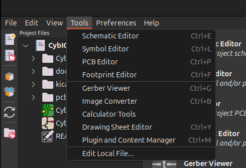
|
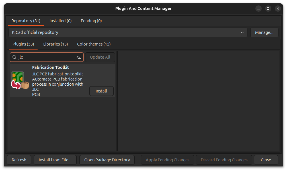
|
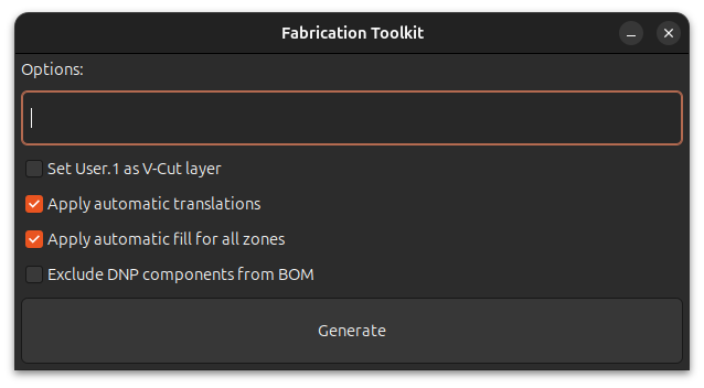
R40 and R46 are marked DNP because their absence is what
encodes hardware v1.1, and the plugin keeps DNP parts out of the CPL
unconditionally but out of the BOM only when this box is ticked. Leave it off
and the two files disagree: JLCPCB's BOM/CPL matching then reports
designators that have no position, which is the failure of #238 with the
files the other way round.
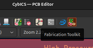
|
|
The toolkit writes hardware/pcb/production/ (gitignored):
CybICS.zip - gerbers and the PTH/NPTH drill filesbom.csv - bill of materials, JLCPCB column layoutpositions.csv - the CPLdesignators.csv, netlist.ipc - not needed by JLCPCBThe plugin ships a CLI, so the set can be regenerated reproducibly -- useful for
checking a change without clicking through the dialog. It needs pcbnew, so run
it in the image CI already uses:
curl -sL https://github.com/bennymeg/Fabrication-Toolkit/archive/refs/tags/5.3.1.tar.gz \
  | tar -xz --one-top-level=ft --strip-components=1
docker run --rm --user $(id -u):$(id -g) -e HOME=/tmp \
  -v "$PWD/ft:/ft" -v "$PWD:/repo" -w /ft setsoft/kicad_auto:ki10 \
  python3 -m plugins.cli -p /repo/hardware/pcb/CybICS.kicad_pcb -t -f -e -nI -nB
-t and -f are the automatic translations and zone fill, which the dialog has
on by default and the CLI does not. -e is the DNP exclusion from step 3. The
plugin reads the board and writes production/; it does not modify the
schematic, the board or the project file.
Whatever route you take, check the two files agree before uploading:
python3 - <<'EOF'
import csv
bom=list(csv.DictReader(open('hardware/pcb/production/bom.csv',encoding='utf-8-sig')))
cpl=list(csv.DictReader(open('hardware/pcb/production/positions.csv',encoding='utf-8-sig')))
b={r.strip() for row in bom for r in row['Designator'].split(',')}
c={r['Designator'] for r in cpl}
print('BOM only:', sorted(b-c) or 'none')
print('CPL only:', sorted(c-b) or 'none')
for x in ('R40','R46','FID1','FID2','FID3'):
    assert x not in b and x not in c, x
print('no DNP or fiducials in either file')
EOFgerber.zipAfter upload, configure the following options:
bom.csv from the production folderpositions.csv from the production folderR40 and R46 are marked DNP -- they encode the hardware revision by
being absent (see Hardware Version Coding).
Confirm they are missing from the uploaded BOM and CPL. Do not take the
plugin's word for it: whether they leave the BOM depends on the checkbox in
step 3, and if JLCPCB places them the board reports code 00000 instead of
00001 and identifies itself as a revision that does not exist.
Every other R41-R44 and R47-R50 must be placed.
After processing, JLCPCB will display component matching:
Review matched components:
For unavailable components:
Verify component orientation:
Use KiCad's 3D viewer to visualize the assembled board:
While this guide focuses on JLCPCB, the PCB can also be ordered from:
Each manufacturer has slightly different processes and pricing. Export files may need adjustment for other manufacturers.
Check the git history for PCB revisions:
git log --oneline -- hardware/pcb/Each revision may have different components or layout. Ensure you're using the latest stable version.
| Qty | Value | Footprint | References |
|---|---|---|---|
| 22 | 1kR | Resistor_SMD:R_0805_2012Metric_Pad1.20x1.40mm_HandSolder | R3, R22, R24, R26, R27, R40, R41, R42, R43, R44, R46, R47, R48, R49, R50, R51 +6 |
| 9 | LED GREEN | LED_SMD:LED_0805_2012Metric_Pad1.15x1.40mm_HandSolder | D2, D4, D8, D11, D12, D13, D15, D17, D19 |
| 8 | 10kR | Resistor_SMD:R_0805_2012Metric_Pad1.20x1.40mm_HandSolder | R28, R29, R30, R31, R32, R33, R34, R35 |
| 8 | 330R | Resistor_SMD:R_0805_2012Metric_Pad1.20x1.40mm_HandSolder | R1, R2, R4, R6, R10, R21, R23, R25 |
| 7 | 0R | Resistor_SMD:R_0805_2012Metric_Pad1.20x1.40mm_HandSolder | R13, R14, R15, R16, R17, R18, R19 |
| 6 | LED RED | LED_SMD:LED_0805_2012Metric_Pad1.15x1.40mm_HandSolder | D1, D5, D6, D14, D16, D18 |
| 3 | 100nF | Capacitor_SMD:C_0805_2012Metric_Pad1.18x1.45mm_HandSolder | C1, C2, C4 |
| 3 | 20kR | Resistor_SMD:R_0805_2012Metric_Pad1.20x1.40mm_HandSolder | R11, R12, R20 |
| 3 | Fiducial | Fiducial:Fiducial_1mm_Mask2mm | FID1, FID2, FID3 |
| 3 | MountingHole | MountingHole:MountingHole_3.2mm_M3 | H1, H2, H3 |
| 2 | 100R | Resistor_SMD:R_0805_2012Metric_Pad1.20x1.40mm_HandSolder | R5, R8 |
| 2 | 5.1kR | Resistor_SMD:R_0805_2012Metric_Pad1.20x1.40mm_HandSolder | R38, R39 |
| 2 | LED WHITE | LED_SMD:LED_0805_2012Metric_Pad1.15x1.40mm_HandSolder | D3, D10 |
| 2 | LED YELLOW | LED_SMD:LED_0805_2012Metric_Pad1.15x1.40mm_HandSolder | D7, D9 |
| 2 | SW_Push | Button_Switch_THT:SW_PUSH_6mm_H5mm | SW1, SW2 |
| 1 | 4.7μF | Capacitor_SMD:C_0805_2012Metric_Pad1.18x1.45mm_HandSolder | C3 |
| 1 | 7*7*5-6P-L WX | cybics:SW-SMD_8P-L7.0-W7.0-P1.40-LS7.4-TL | SW3 |
| 1 | Conn_01x03_Pin | Connector_PinHeader_2.54mm:PinHeader_1x03_P2.54mm_Vertical | J2 |
| 1 | Conn_01x05_Pin | Connector_PinHeader_2.54mm:PinHeader_1x05_P2.54mm_Vertical | J3 |
| 1 | R_Potentiometer | Potentiometer_SMD:Potentiometer_Bourns_3314J_Vertical | RV1 |
| 1 | Raspberry_Pi_2_3 | Module:Raspberry_Pi_Zero_Socketed_THT_FaceDown_MountingHoles | J1 |
| 1 | STM32G070RBTx | Package_QFP:LQFP-64_10x10mm_P0.5mm | U1 |
| 1 | USB_C_Receptacle_USB2.0 | Connector_USB:USB_C_Receptacle_G-Switch_GT-USB-7010ASV | J4 |
| 1 | WC1602A/HD44780 | Display:WC1602A | DS1 |
The 91 most common of 92 parts.
cardonabits/haxo-hw
Haxophone, an electronic musical instrument that resembles a saxophone

Allen-Synthesis/EuroPi
EuroPi: A reprogrammable Eurorack module based on the Raspberry Pi Pico

mmccoyd/hillside
Family of split ergonomic keyboards with three rows of six or five keys and a generous thumb arc

ChrisChrisLoLo/keezyboost40
4x10 ortholinear with an LCD in the middle. Uses the Raspberry Pi Pico, as well as Rust firmware

nodestark/mdb-esp32-cashless
ESP32-based MDB cashless device for vending machines, supporting EVA DTS DEX/DDCMP telemetry and payments over the MDB protocol via Bluetooth and MQTT


cnlohr/cnhardware
My dumping grounds for all my kicad projects and random hardware bringup.
It measures 160 × 100 mm and has 2 copper layers, 1.6 mm thick.
92 parts. The full list of its parts is on this page, with links to each part's symbol and footprint where PCBKit's library has them.
From the mniedermaier/CybICS repository on GitHub, at the commit this page was made from: the board is hardware/pcb/CybICS.kicad_pcb and its schematic hardware/pcb/CybICS.kicad_sch. PCBKit opens the board in the browser, with nothing to install.
Its repository publishes it under the MIT licence: you may reuse it on that licence's terms (keep the author's notice, and for a copyleft licence share your changes alike).