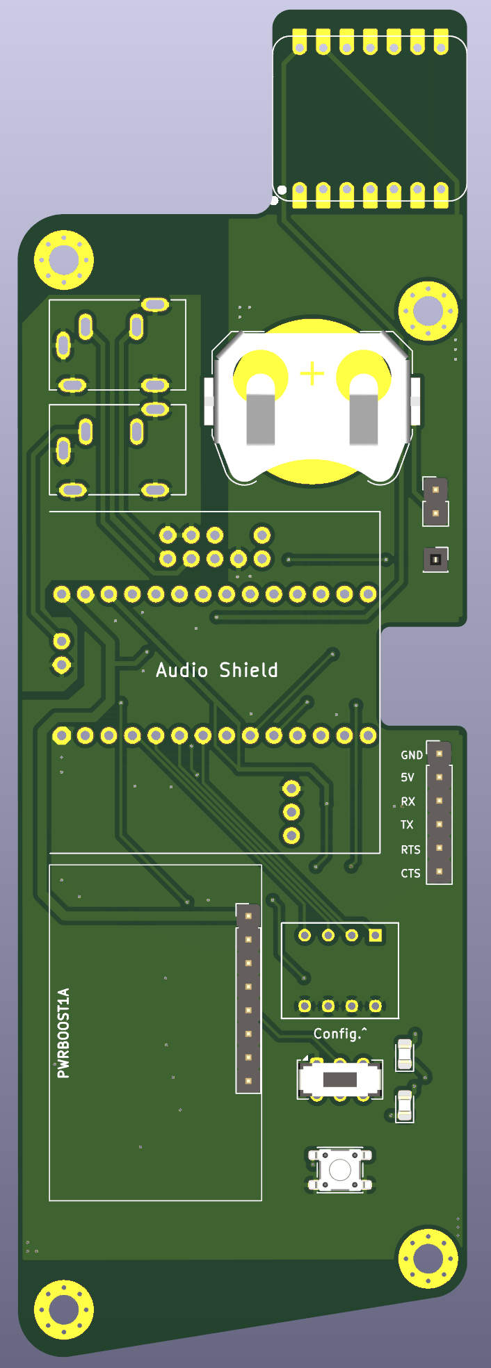
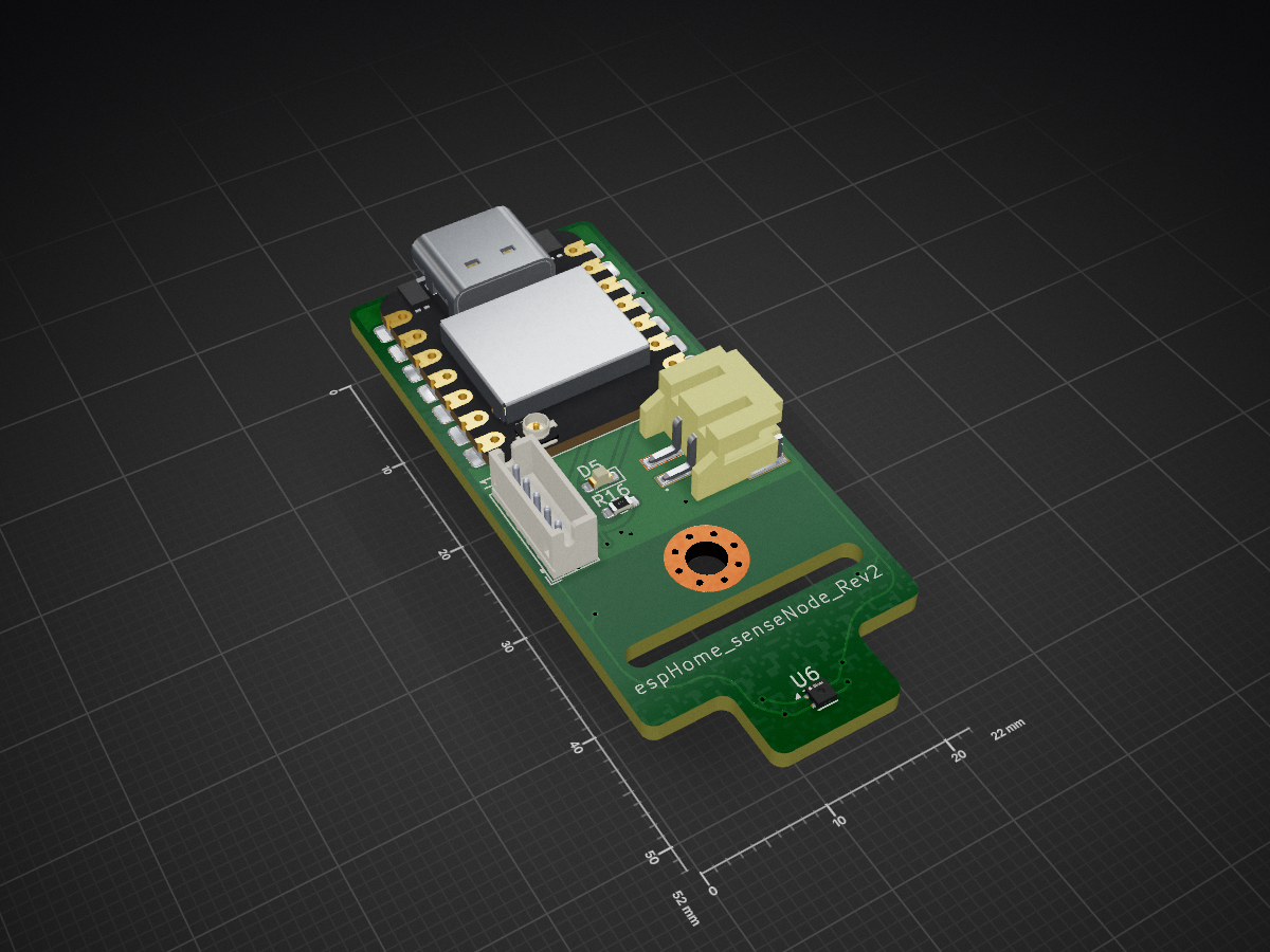
XIAO AUDIO is an open-source printed circuit board by mmontee, from the mmontee/nrf52840_openWSN_sensor_node repository on GitHub, published under the MIT licence. It is a 2-layer board of 22 × 52 mm with 39 parts on 40 nets, routed with 242 tracks and 37 vias.
It is built around the AP62150Z6, ENS160-BGLT and BQ25185DLHR, with the NSR0320MW2 and S2B-PH-SM4-TB among its other parts. Its parts include 12 resistors, 9 capacitors, 5 ICs, 4 diodes and 3 connectors. It belongs with the audio and music and sensors and measurement boards of this library.
This project builds upon the foundation of the West_Lab_Hydrophone_Data_Logger. The initial objective was to integrate the nRF52840 into the existing hardware architecture, with the long-term goal of migrating all signal processing tasks from the Teensy 4.0 to the nRF52840. This consolidation of processing onto a single microcontroller is expected to yield significant power savings while decreasing the complexity, size, and cost of each sensor node.
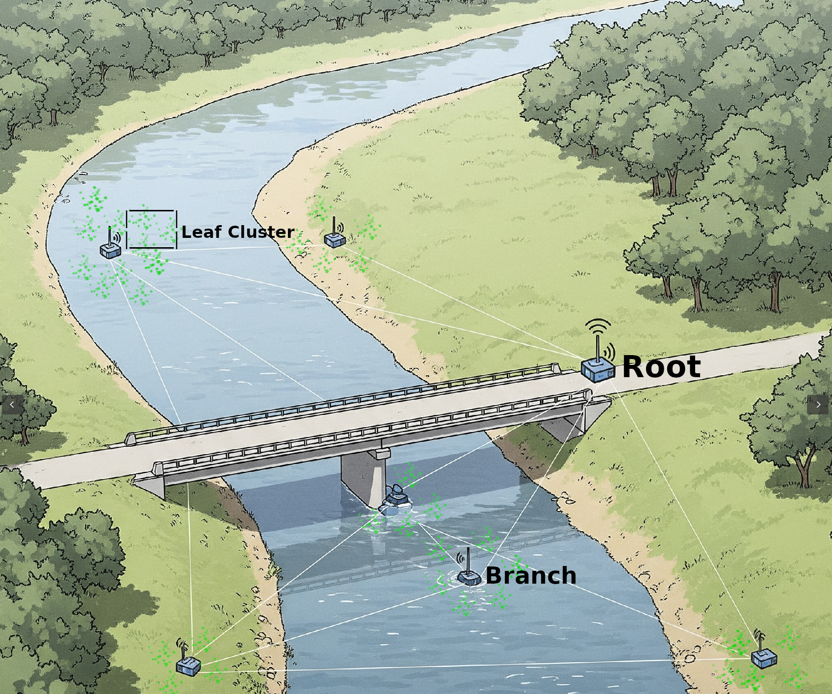
The ultimate aim is to create a wireless acoustic sensor network using the XIAO nRF52840 and OpenWSN. In the current transitional phase, a Teensy 4.0 with a Teensy Audio Adaptor Board captures and processes acoustic signals, and samples are saved to an SD card. The output is passed through the wireless network to a central root node. This root node does not perform sensing; instead, it passes information to an LTE-M modem, which uses MQTT to send the processed data to a cloud storage solution.
A critical aspect of the final transition will be to incorporate appropriate signal conditioning hardware to replace the functionality of the Teensy Audio Adaptor Board.
Current Software Status
Complete:
Hardware Programming: Established a method to program the device with OpenWSN.
Port OpenWSN to XIAO: Modified the existing OpenWSN project for the nRF52840-DK to support the XIAO.
Modified Openserial Driver: Adapted the openserial driver to enable UART communication between the Teensy and the nRF52840.
ADC Driver: Developed a dedicated ADC driver for the nRF52840's SAADC peripheral.
ADC Application: Created a sample application to demonstrate the driver's functionality and provide a foundation for future signal processing work.
Incomplete:
Signal Capture and Processing on nRF52840: Expand the ADC application to capture and process a time series of samples directly on the XIAO nRF52840.
Teensy 4.0 OpenWSN Output Parse Program: Procure a new LTE-M modem and continue testing/development.
Current Hardware Status
Complete:
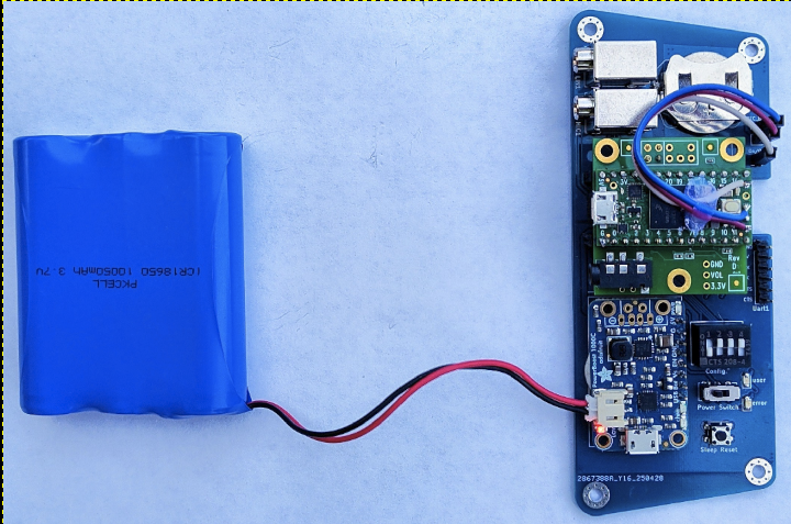
Each sensor node consists of a custom PCB that interfaces the XIAO nRF52840, Teensy boards, RTC battery, a battery management board, and various I/O.
The existing West Lab Hydrophone Data Logger with an LTE-M modem.
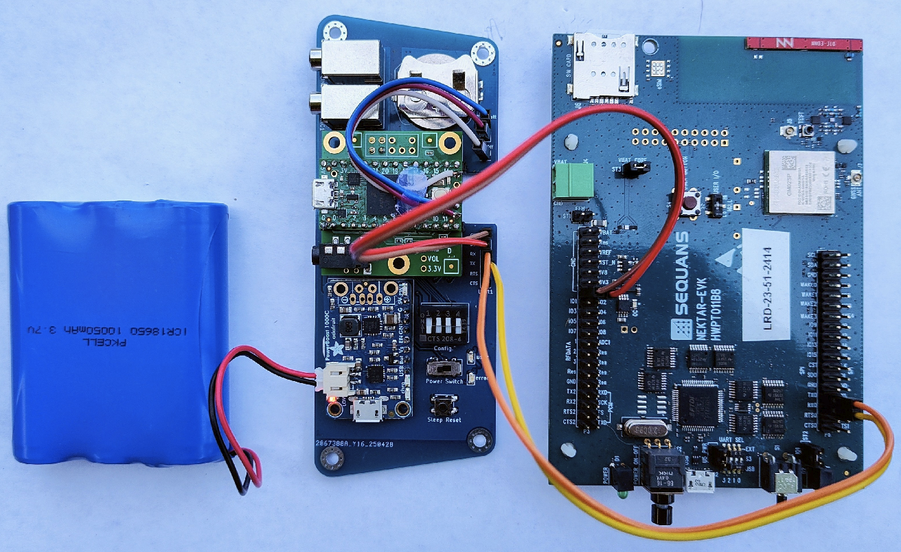
Shown below is the "West_Lab_Hydrophone_Data_Logger" PCB modified to include the XIAO nRF52840.
Incomplete:
A new PCB revision that incorporates signal conditioning hardware and removes the Teensy 4.0 and its audio adapter board.
Battery Life Analysis
This section uses average current consumption measurements made with a JouleScope to estimate battery life.
Current consumption measurements were generated by attaching the JouleScope and allowing a device to run in a particular mode for over one minute. The resulting statistical average current consumption generated by the JouleScope software was recorded.
Data Logger Node
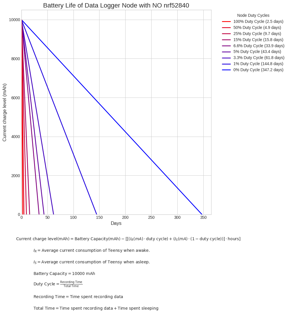
Battery life estimates for the data logger without the XIAO nRF52840.
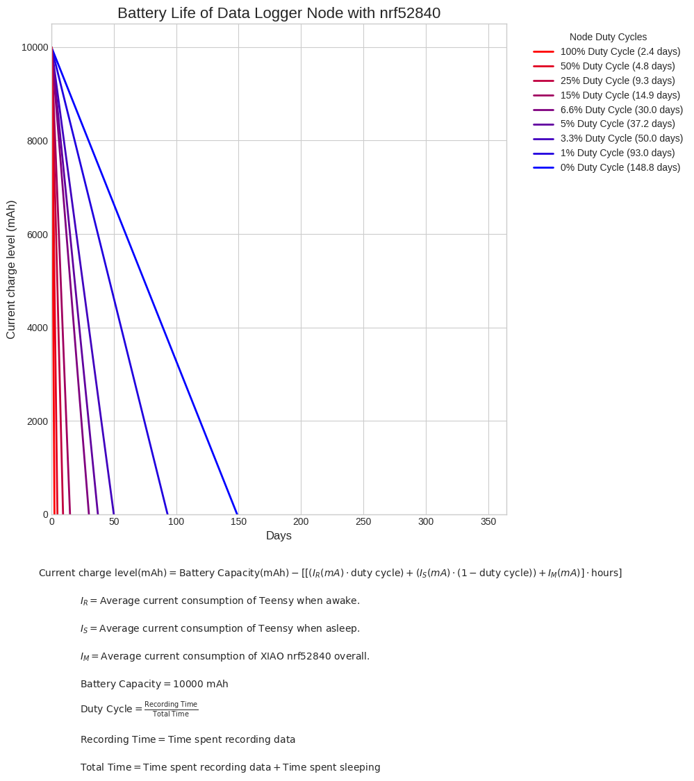
Battery life estimates for the data logger with the XIAO nRF52840.
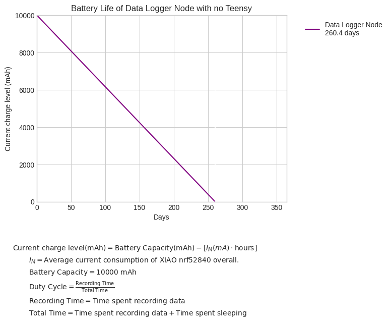
Battery life estimates for a data logger with only the XIAO nRF52840 (Teensy 4.0 and Audio Adaptor Board removed).
Root Node
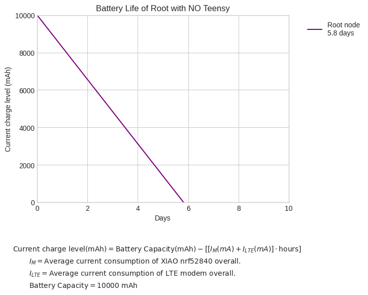
Battery life estimates for the root node without a Teensy 4.0.
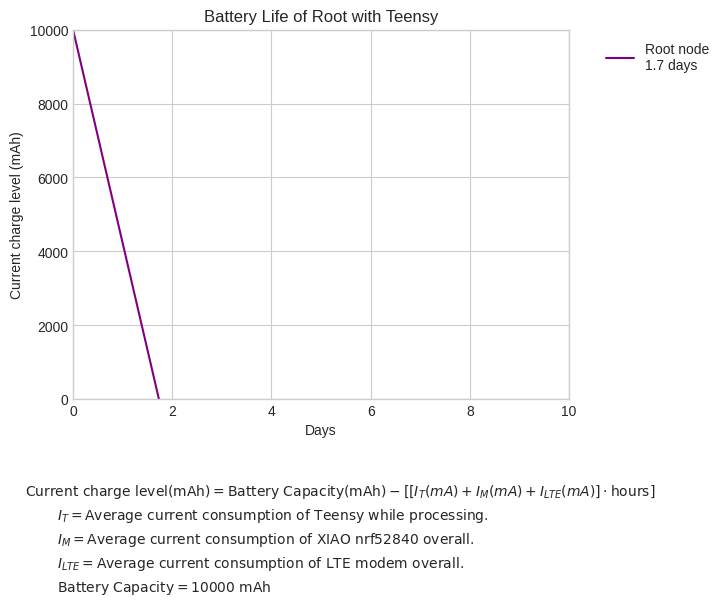
Battery life estimates for the root node with a Teensy 4.0.
Conclusion
The integration of the XIAO nRF52840 wireless mote introduces a significant power cost, primarily during idle periods.
Impact at Operational Duty Cycle: At the target operational duty cycle of 6.6%, adding the nRF52840 reduces the battery life from 33.4 days to 30.0 days. This loss of only 3.4 days is a reasonable trade-off for gaining wireless mesh networking capabilities.
Idle Power is Key: The nRF52840's idle power consumption is its largest drawback. At a 0% duty cycle, its presence cuts the node's standby time by more than half, from 347 days to 149 days.
High-Duty Cycle Operation: As the data recording frequency increases, the power consumption of the Teensy processor becomes the dominant factor, and the relative impact of the nRF52840 diminishes.
Ultra-Low Power Potential: A simplified sensor node consisting of only the XIAO nRF52840 demonstrates the potential for extremely long-term deployments, lasting an estimated 260 days on the same 10,000 mAh battery.
ssss
Root Node: Designed for Function over Efficiency
The Root Node hardware is configured for constant availability and processing power rather than battery longevity. Its battery life is extremely limited.
Primary Power Drain: The largest power consumers are the always-on LTE modem and the Teensy processor. A base configuration with just the modem and nRF52840 lasts only 5.8 days.
Teensy's High Cost: Adding the always-on Teensy for data processing is the single largest power draw, reducing the battery life by over 70% to just 1.7 days.
Recommendations: For any practical deployment, the Root Node requires a continuous power source (e.g., mains or solar). Significant power savings could be achieved through future hardware and software revisions, such as implementing a sleep mode for the Teensy and power-cycling the LTE modem between scheduled transmissions.
Guide for OpenWSN on XIAO nRF52840
Fortunately, foundational work has been completed in OpenWSN's nRF52840-DK implementation, which can be found in the develop_FW-893 branch. In this project, the nRF52840-DK is used as a programmer and debugger for the XIAO nRF52840 board.
This guide will step through the processes of:
Configuring the existing OpenWSN project for the XIAO nRF52840's pinout.
Using the nRF52840-DK to program and debug the XIAO nRF52840.
Using UART to transmit information to and from an OpenWSN application.
This guide assumes you have the following hardware:
Clone the OpenWSN firmware repository: git clone https://github.com/openwsn-berkeley/openwsn-fw
Switch to the correct branch: git checkout develop_FW-893
Navigate to the project folder: cd openwsn-fw/projects/nrf52840-DK/
Open the project file:nrf52840_dk.emProject
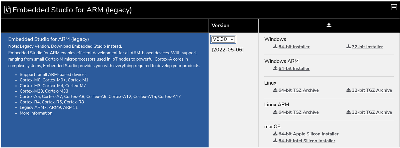
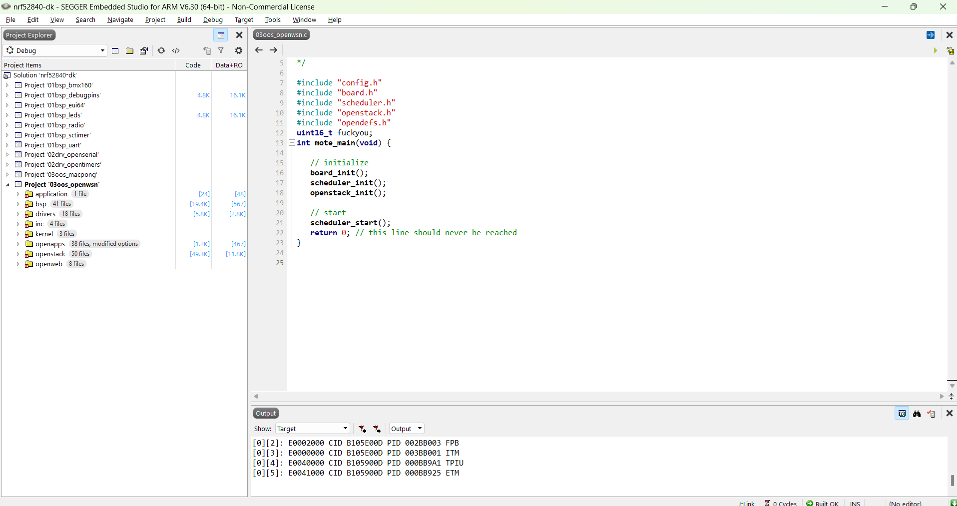
The project should open in the Segger Embedded Studio IDE installed in the first step.
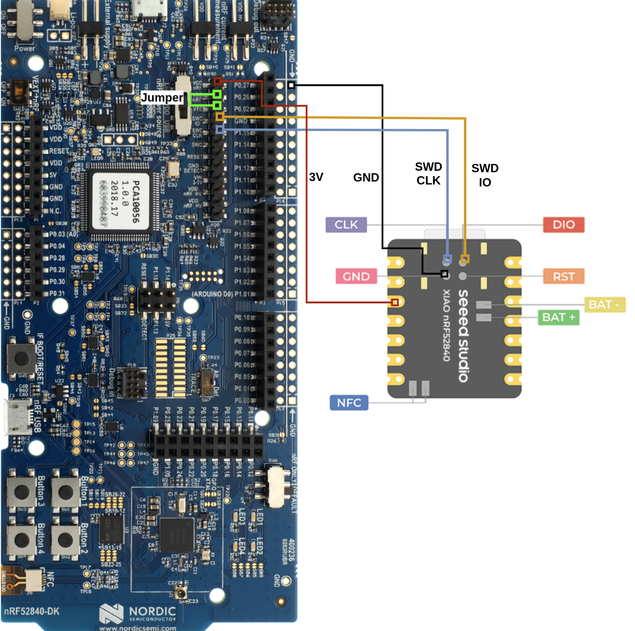
Connecting the XIAO nRF52840 to the nRF52840-DK
Programming is done via the JTAG/SWD interface on the nRF52840-DK, which is exposed through the onboard J-Link debugger.
Both boards must share a common ground reference.
Power must be provided to both boards (in this guide, the nRF52840-DK powers the XIAO nRF52840).
Connect SWD CLK.
Connect SWD IO.
Connect the jumper to enable the onboard debugger.
The connections are illustrated below.
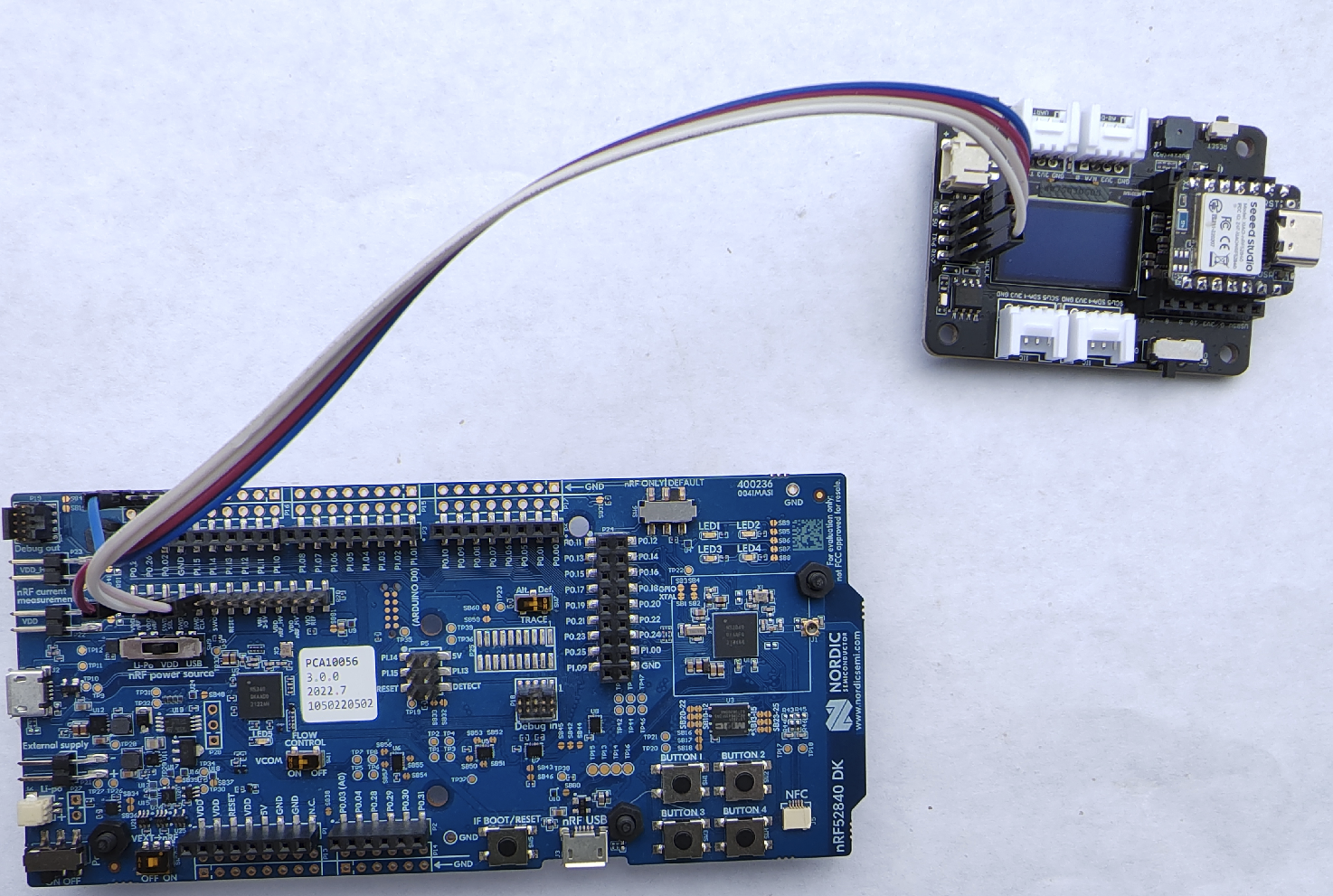
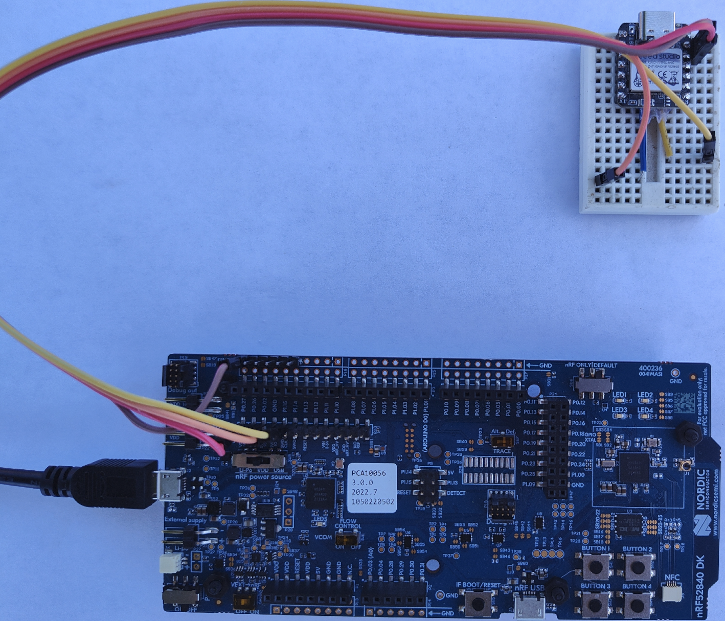
We created the necessary connections using two methods:
Using the "Expansion Board Base for XIAO": This board provides pogo pin contacts for the XIAO nRF52840's SWD pads, simplifying the connection process.
Soldering wires directly: Alternatively, wire leads can be soldered to the XIAO nRF52840's SWD pads. The leads can then be connected directly to the nRF52840-DK as shown below.
Modifying OpenWSN for the XIAO nRF52840
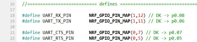
Two changes must be made to the firmware to configure it for the XIAO nRF52840 platform: the UART and LED pin assignments must be updated.
The UART pin assignments are found in bsp/uart.c. The image below shows the correct values for the XIAO nRF52840.
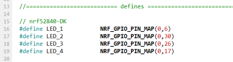
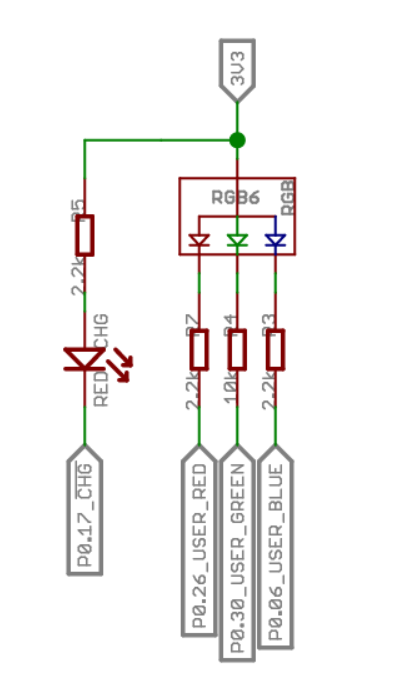
The LED pin assignments must be changed in bsp/leds.c. The image below shows the correct values for the XIAO nRF52840.
Reference the schematic for LED pin assignments:
Programming the XIAO nRF52840
Assuming the necessary connections are established between the XIAO nRF52840 and the nRF52840-DK:
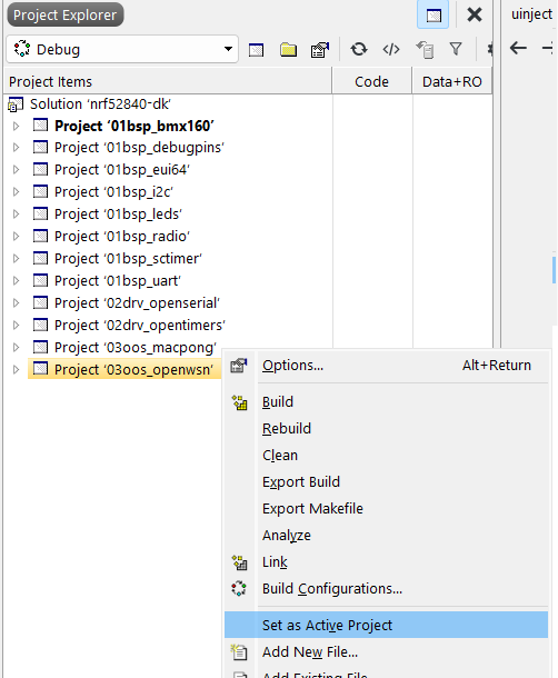
Set 03oos_openwsn as the active project by right-clicking its name in the "Project Explorer".
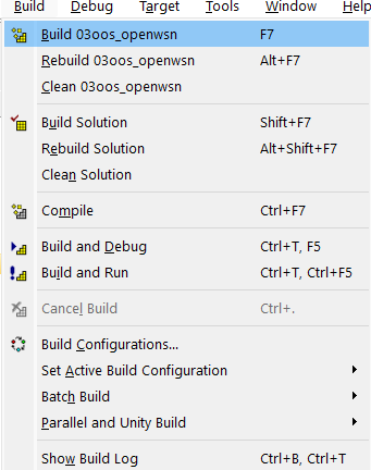
Compile the project: Build -> Build 03oos_openwsn.
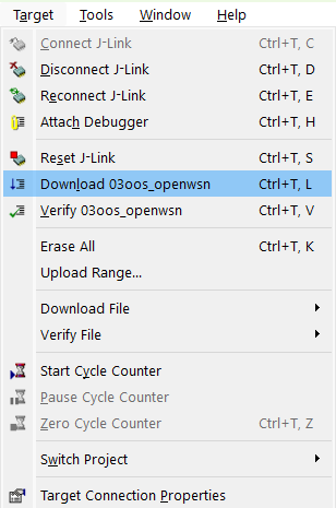
Program the device: Target -> Connect J-Link, then Target -> Download 03oos_openwsn.
Guide for UART Communication with OpenWSN on XIAO nRF52840
This project modifies openserial.c to execute functions when specific UART messages are received. Sensor nodes receive processed signal information from an external source (like the Teensy) and pass this data to the root node. The root node's UART output is then parsed by another device.
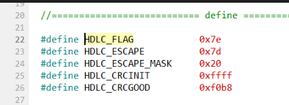
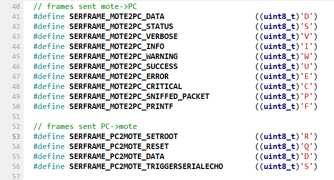
Incoming UART messages are parsed within openserial.c using a set of flags from openhdlc.h and command characters (cmdByte) defined in openserial.h, as shown below.
Flags
cmdBytes
Valid messages must be preceded by an HDLC_FLAG, begin with a valid command byte, contain the payload, and be terminated with a second HDLC_FLAG.
A message coming into openserial should have the form: <HDLC_FLAG><cmdByte><payload><HDLC_FLAG>
We send information into the node using the following format, where '~' is the HDLC_FLAG, 'D' is the cmdByte, and '1234567890' is example data:
Example: ~D1234567890~
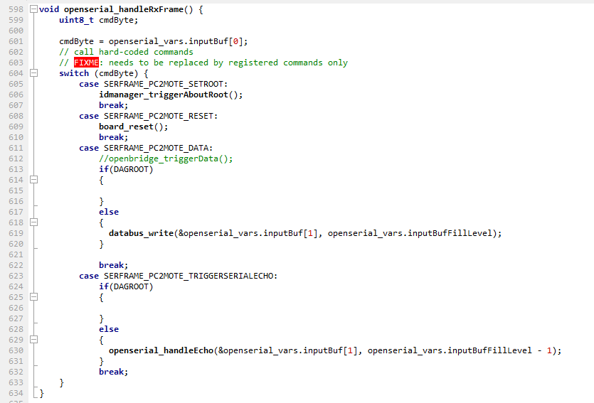
After a valid message is parsed, it is passed to a switch statement that acts on the received cmdByte. This byte triggers a specific action. Below, the code passes the incoming data as that action or does nothing if the node is the root.
Once the data is on the data bus, it can be read by a custom application (e.g., `uinject`) that will create a UDP packet containing the data to be passed over the network.
ADC Driver for nRF52 SAADC (XIAO nRF52840)
1. Overview
This document describes a low-level driver for the nRF52 Successive-Approximation Analog-to-Digital Converter (SAADC) peripheral. The driver is designed for simplicity and provides a blocking (synchronous) API for single-channel ADC conversions.
It is specifically tailored with pin definitions corresponding to the analog pins on the Seeed Studio XIAO nRF52840 board but can be adapted for other nRF52-based hardware.
Key Features
Easy Configuration: Uses a single configuration structure (adc_config_t) to set all major parameters.
Blocking Sampling: The adc_sample() function waits for the conversion to complete before returning, simplifying application logic.
Hardware Abstraction: Maps XIAO nRF52840 pin names (A0-A5) to the correct nRF52 AIN inputs.
Configurable Parameters:
Resolution (8, 10, 12, 14-bit)
Hardware Oversampling (up to 256x)
Reference Voltage (Internal 0.6V or VDD/4)
Input Gain (1/6x to 4x)
Acquisition Time (3µs to 40µs)
Automatic Calibration: Performs an automatic offset calibration during initialization to improve accuracy.
2. API Reference
The driver exposes three main functions for controlling the ADC.
void adc_init(const adc_config_t* config)
Initializes the SAADC peripheral with the specified settings. This function must be called before any sampling can occur.
Description: Configures the ADC resolution, oversampling, channel settings (pin, gain, reference, acquisition time), performs an offset calibration, and enables the peripheral.
Parameters:
config: A pointer to a constant adc_config_t structure containing the desired ADC settings.
bool adc_sample(uint16_t* result)
Performs a single, blocking ADC conversion on the channel configured during initialization.
Description: This function starts the ADC, triggers a sample, and waits for the EVENTS_END interrupt flag. It then copies the conversion result from the internal buffer to the user-provided location. To save power, it stops the ADC after the sample is complete.
Warning: This function blocks program execution until the conversion is complete.
Parameters:
result: A pointer to a uint16_t variable where the ADC conversion result will be stored. The value's range depends on the configured resolution (e.g., 0-1023 for 10-bit).
Returns:
true: If the conversion was successful.
false: If the ADC was not initialized or the result pointer is NULL.
void adc_uninit(void)
Disables and powers down the SAADC peripheral to save energy.
Description: Stops any ongoing conversions, disables the peripheral, and resets channel configurations. An adc_init() call is required before any new samples can be taken.
3. Configuration
Configuration is handled via the adc_config_t struct and several enum types.
adc_config_t Structure
This structure holds all the necessary parameters for the adc_init function.
ADC_REFERENCE_VDD_DIV_4: Uses VDD / 4 as the reference.
adc_gain_t
Sets the gain for the internal pre-amplifier. The total input voltage range is determined by V_Reference / Gain.
Enum Value
Gain
Input Range (with 0.6V VREF)
Input Range (with VDD/4 VREF)
ADC_GAIN_1_6
1/6x
0 - 3.6V
0 - 6.0V (e.g., if VDD=3.3V → 0-4.95V)
ADC_GAIN_1_5
1/5x
0 - 3.0V
0 - 5.0V (e.g., if VDD=3.3V → 0-4.125V)
ADC_GAIN_1_4
1/4x
0 - 2.4V
0 - 4.0V (e.g., if VDD=3.3V → 0-3.3V)
ADC_GAIN_1_3
1/3x
0 - 1.8V
0 - 3.0V (e.g., if VDD=3.3V → 0-2.475V)
ADC_GAIN_1_2
1/2x
0 - 1.2V
0 - 2.0V (e.g., if VDD=3.3V → 0-1.65V)
ADC_GAIN_1
1x
0 - 0.6V
0 - 1.0V (e.g., if VDD=3.3V → 0-0.825V)
ADC_GAIN_2
2x
0 - 0.3V
0 - 0.5V (e.g., if VDD=3.3V → 0-0.4125V)
ADC_GAIN_4
4x
0 - 0.15V
0 - 0.25V (e.g., if VDD=3.3V → 0-0.206V)
Note: The actual input voltage range is limited by VDD. For example, with ADC_GAIN_1_6 and VDD at 3.3V, the effective input range is 0V to 3.3V. The most common setting for measuring a voltage from 0 to VDD (e.g., 3.3V) is to use ADC_REFERENCE_INTERNAL and ADC_GAIN_1_6.
adc_acqtime_t
Sets the acquisition time for the sample-and-hold capacitor. Longer times are needed for high-impedance sources.
ADC_ACQTIME_3US
ADC_ACQTIME_5US
ADC_ACQTIME_10US
ADC_ACQTIME_15US
ADC_ACQTIME_20US
ADC_ACQTIME_40US
4. Usage Example
Here is a complete example of how to initialize, configure, and read from an analog pin.
c
#include"adc.h"
#include <stdio.h> // For printingint main(void){// 1. Configure the ADC// This example configures the ADC to read a voltage between 0-3.6V// on pin A0 with 10-bit resolution.const adc_config_t my_adc_config = {
.resolution = ADC_RESOLUTION_10BIT,
.oversample = ADC_OVERSAMPLE_4X, // Use 4x oversampling for better stability
.reference = ADC_REFERENCE_INTERNAL, // Use internal 0.6V reference
.gain = ADC_GAIN_1_6, // Use 1/6 gain (effective input range is 0.6V * 6 = 3.6V)
.acq_time = ADC_ACQTIME_10US,
.pin = ADC_PIN_A0
};
// 2. Initialize the ADC
adc_init(&my_adc_config);
// 3. Main loop to sample the ADCwhile(1){uint16_t adc_raw_value;
OpenWSN ADC Reader Application
1. Overview
This document describes adcread, a simple application component for the OpenWSN operating system. Its purpose is to periodically read an analog sensor using the adc driver and make the latest reading available to other parts of the system.
The application integrates with the OpenWSN kernel's opentimers service to schedule non-blocking, periodic ADC sampling. This makes it an efficient, low-power way to monitor a sensor.
Key Features
OpenWSN Integration: Built as a standard OpenWSN component that uses the kernel's timer service for scheduling.
Periodic Sampling: Automatically reads the configured ADC channel every 5 seconds (ADC_READER_PERIOD_MS).
Non-blocking API: Provides a simple, non-blocking function (adcread_get_value()) for other modules to retrieve the latest sensor data.
Power Efficient: The application is designed not to run on the DAGroot to save energy on the most critical node in the network.
Driver Abstraction: Uses the underlying adc peripheral driver, separating the application logic from the hardware-specific details.
2. API Reference
The adcread application exposes two public functions.
void adcread_init(void)
Description: This function configures and initializes the underlying adc driver with static settings defined within adcread.c. It then creates and schedules a periodic timer that will trigger an ADC reading.
Warning: This function must be called afteropentimers_init() has been successfully executed.
uint16_t adcread_get_value(void)
Description: This is a non-blocking function that immediately returns the most recent ADC value stored by the periodic timer task. It does not trigger a new ADC reading.
Returns: A uint16_t representing the latest raw ADC conversion result.
3. Configuration
Unlike the driver, the application's configuration is hard-coded within the adcread.c file for simplicity. To change these settings, you must edit the source file and recompile.
Default ADC Configuration
The following settings are applied in adcread_init():
The sampling rate is controlled by a preprocessor macro:
c
// Defines the period for reading the ADC in milliseconds
#define ADC_READER_PERIOD_MS 5000// Read ADC every 5 seconds
4. Integration with OpenWSN
Here is how to integrate and use the adcread application within the OpenWSN framework.
1. Initialization
Call adcread_init() from the main system initialization function (e.g., in openwsn.c's openwsn_init function), ensuring it is called after the kernel services are available.
// In openwsn.c or your main application file
#include "adcread.h"
void openwsn_init(void) {
// ... other initializations
board_init();
scheduler_init();
opentimers_init();
// ... other initializations
text
// Initialize the ADC reader application
adcread_init();
// ... more initializations
scheduler_start();
}
2. Retrieving Data
Other application modules (e.g., a data packet creation module like `C6T` or a custom application) can get the latest sensor data by calling adcread_get_value().
// Example in another module that needs the sensor data
#include "adcread.h"
// Get the latest value from the ADC reader app
sensor_value = adcread_get_value();
// Now, 'sensor_value' can be added to a packet payload
// to be sent over the 6LoWPAN network.
// ...
}
3. Component ID
For error logging via openserial_printLog, ensure that COMPONENT_ADCREAD is defined in the opendefs.h file alongside other component IDs.
For certain applications, you might need to capture a rapid burst of samples. The following method uses a blocking loop to monopolize the CPU and capture samples as fast as the hardware allows, without yielding control to the OpenWSN scheduler.
Using a blocking loop in a cooperative OS like OpenWSN is dangerous and should be handled with extreme care.
Processor Hogging: The loop will prevent all other tasks from running, including the OpenWSN scheduler and the 6TiSCH network stack.
Network Instability: If the total time spent in the blocking loop is longer than a network timeslot (typically a few milliseconds), the node will fail to communicate. This can cause it to lose synchronization with the network, leading to packet loss or complete disconnection.
When to Use: This method is only acceptable for very short bursts where the total capture time is guaranteed to be minimal (e.g., less than one millisecond). For any longer duration, a non-blocking, task-based approach is required to maintain system stability.
Capturing a Burst with a Blocking Loop
This is achieved by creating a function that enters a tight `for` loop, calling `adc_sample()` in each iteration.
1. Define buffer and state variables:
First, define the buffer size in adcread.c and add necessary state variables to `adcread_vars_t`.
typedef struct {
opentimers_id_t timer_id;
uint16_t        latest_adc_value;
adc_config_t    adc_config;
bool            initialized;
// --- New variables for burst mode ---
uint16_t        burst_buffer[ADC_BURST_BUFFER_SIZE]; // Buffer for samples
bool            burst_in_progress;                   // Flag to prevent re-entrant calls
} adcread_vars_t;
2. Create the blocking capture function:
This function will contain the blocking loop. After the capture is complete, it schedules a separate, non-blocking task to process the data, which is a safer way to handle potentially long computations.
// adcread.c -- function prototypes
void _adcread_process_task_cb(void); // Task to process data after capture
void adcread_capture_burst_blocking(void); // Public function to initiate a burst
// Public function with the blocking capture loop
void adcread_capture_burst_blocking(void) {
if (!adcread_vars.initialized || adcread_vars.burst_in_progress) {
return; // Exit if not ready or another burst is active
}
adcread_vars.burst_in_progress = true;
text
// Stop the periodic timer to prevent interference
opentimers_stop(adcread_vars.timer_id);
// --- START OF BLOCKING SECTION ---
// This loop takes full control of the CPU. No other tasks will run.
for (uint16_t i = 0; i < ADC_BURST_BUFFER_SIZE; i++) {
adc_sample(&adcread_vars.burst_buffer[i]);
}
// --- END OF BLOCKING SECTION ---
// Now that the time-critical capture is done, schedule a
// non-blocking task to process the data.
scheduler_push_task(_adcread_process_task_cb, TASKPRIO_ADC);
adcread_vars.burst_in_progress = false;
// Restart the periodic timer for normal operation
opentimers_scheduleIn(
adcread_vars.timer_id,
ADC_READER_PERIOD_MS,
TIME_MS,
TIMER_PERIODIC,
_adcread_timer_cb
);
}
On-Mote Data Processing
Sending a large buffer of raw samples over the network is inefficient. Processing the data on the mote first and transmitting only the result reduces network traffic and saves energy. The `_adcread_process_task_cb` function is the ideal place for this computation, as it runs as a standard, non-blocking OpenWSN task.
A comprehensive, multi-sensor IoT telemetry dashboard built around the Freenove ESP32-WROOM development board. This custom KiCad printed circuit board (PCB) integrates precision environmental sensing, analog ambient…
It measures 22 × 52 mm and has 2 copper layers, 1.6 mm thick.
What parts does the XIAO AUDIO use?
39 parts, built around the AP62150Z6, ENS160-BGLT, BQ25185DLHR and NSR0320MW2. The full list of its parts is on this page, with links to each part's symbol and footprint where PCBKit's library has them.
Where can I download the XIAO AUDIO KiCad files?
From the mmontee/nrf52840_openWSN_sensor_node repository on GitHub, at the commit this page was made from: the board is Hardware/XIAO_AUDIO/XIAO_AUDIO.kicad_pcb and its schematic Hardware/XIAO_AUDIO/XIAO_AUDIO.kicad_sch. PCBKit opens the board in the browser, with nothing to install.
Can I use the XIAO AUDIO design in my own project?
Its repository publishes it under the MIT licence: you may reuse it on that licence's terms (keep the author's notice, and for a copyleft licence share your changes alike).

 mmontee/nrf52840_openWSN_sensor_node