
8 layers60 × 70 mm
 mlab-modules/FRAM012
8 Mbit FRAM (CY15B108QN) fast data write, low power consumption, and high radiation resistance data storage
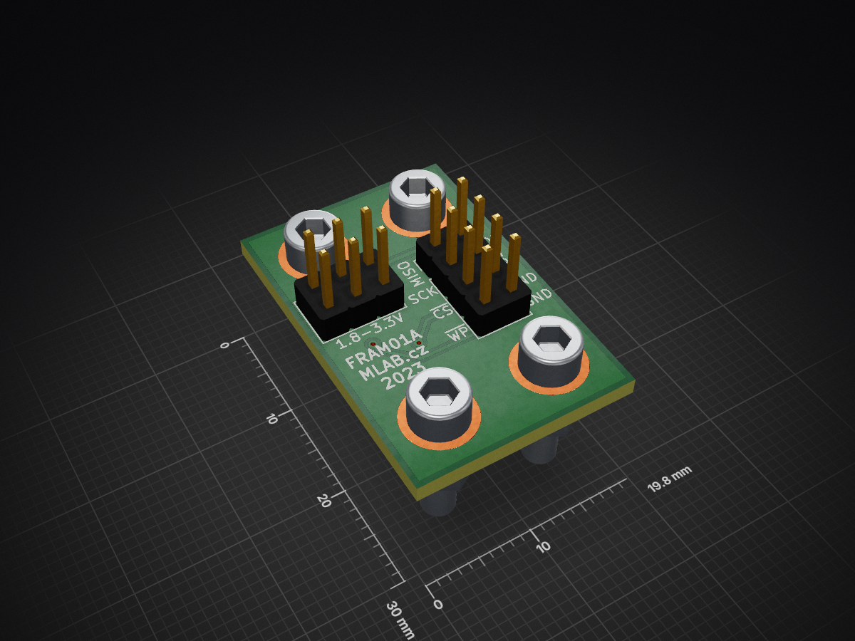
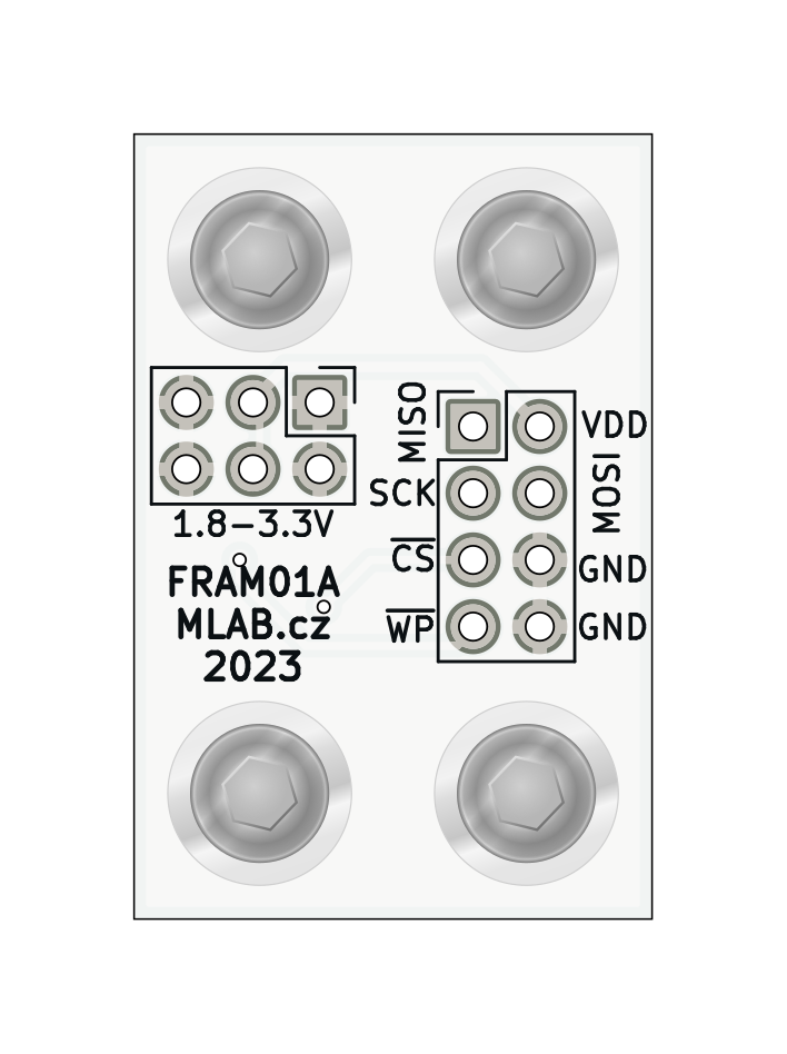
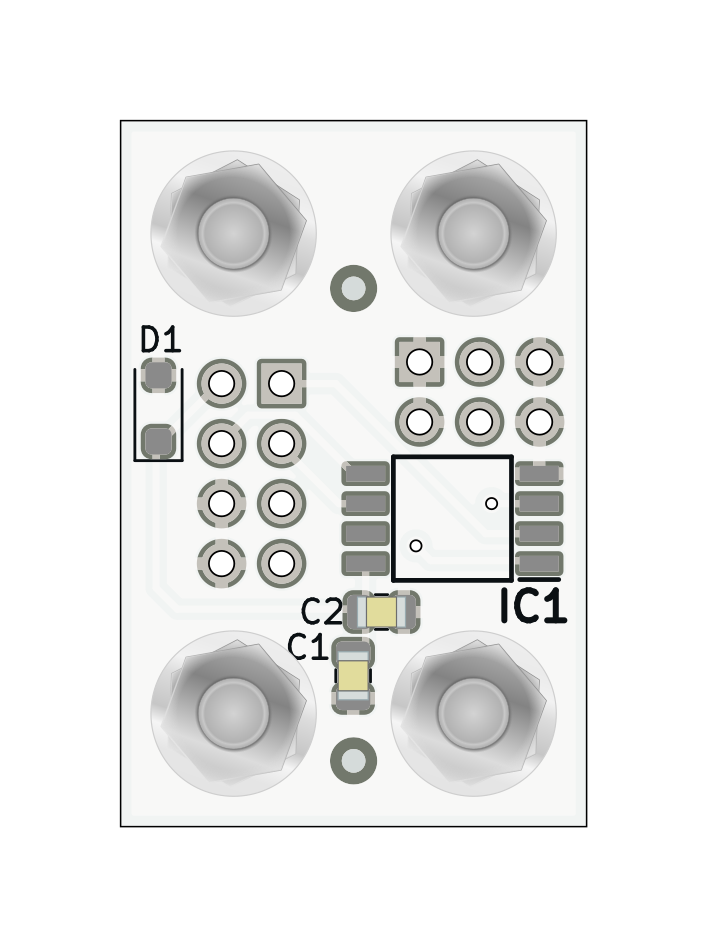
FRAM01 is an open-source printed circuit board by mlab-modules, from the mlab-modules/FRAM01 repository on GitHub, published under the GPL-3.0 licence. It is a 2-layer board of 19.8 × 30 mm with 12 parts on 8 nets, routed with 29 tracks and 2 vias.
It is built around the CY15B108QN-40SXI. Its parts include 2 capacitors, 2 connectors, 1 IC and 1 diode.
The MLAB module with FRAM (Ferroelectric Random Access Memory) CY15B108QN provides a unique combination of features that outperform traditional forms of non-volatile memories such as Flash or EEPROM.
FRAM, also known as Ferroelectric Random Access Memory, offers a range of key advantages that differentiate it and make it suitable for various applications:
Fast data write: FRAM allows fast data write with speeds comparable to the read speed. This property is much faster than writing data to Flash or EEPROM memories.
Low power consumption: The process of writing to FRAM requires less energy than writing to Flash or EEPROM memories due to high speed.
Very high write/read cycles: FRAM can undergo approximately 10¹⁵ write and read cycles, which is much more than other forms of non-volatile memories.
High radiation resistance: Due to its unique physical operation principle, FRAM is more resistant to radiation than other types of memories. The ferroelectric material used to store data can hold an electrical charge without the need for power. This means that once a bit is written to a memory cell, it stays there until something physically changes it. This property, known as polarization, allows FRAM to resist ionizing radiation that can cause random changes in the value of the charge in other types of memories.
For a more comprehensive understanding of FRAM, you can refer to the FRAM Wikipedia page.
Thanks to these unique properties, FRAM is suitable for a range of applications, including:
Industrial automation: For quick data logging and applications that require a large number of writes.
Energy measurement: Where there is a need to write data quickly and frequently with low energy consumption.
Automotive applications: FRAM is resistant to radiation and temperature fluctuations, making it ideal for use in the automotive industry.
Aerospace and defense applications: Thanks to its resistance to ionizing radiation, FRAM is an ideal choice for applications that are exposed to high levels of radiation.
For detailed information on CY15B108QN FRAM memory, please refer to the datasheet.
This module is perfectly tailored for demanding applications that require high write speed, high reliability and durability, and low power consumption. Take advantage of the benefits of FRAM memory in the MLAB module with CY15B108QN.

The MLAB modules provide a standard for developing modular solutions. They offer versatile usage as they can be either standalone modules for specific tasks or used as building blocks for more complex systems. The compact form factor along with the robust design of the MLAB modules ensures their effectiveness in a variety of applications. The MLAB system contains a wide range of electronic modules, each serving a specific function, which allows for great flexibility in designing electronic systems.
| Qty | Value | Footprint | References |
|---|---|---|---|
| 2 | Fiducial | Fiducial:Fiducial_1mm_Mask2mm | FID1, FID2 |
| 2 | HOLE | Mlab_Mechanical:MountingHole_3mm | M3, M4 |
| 2 | HOLE M3 | Mlab_Mechanical:MountingHole_3mm | M1, M2 |
| 1 | 100nF | Capacitor_SMD:C_0805_2012Metric | C2 |
| 1 | 10uF | Capacitor_SMD:C_0805_2012Metric | C1 |
| 1 | BZT52H-C3V6,115 | Diode_SMD:D_SOD-123F | D1 |
| 1 | CY15B108QN-40SXI | KiCad:SOIC127P800X203-8N | IC1 |
| 1 | HEADER_2x03_PARALLEL | Connector_PinHeader_2.54mm:PinHeader_2x03_P2.54mm_Vertical | J1 |
| 1 | HEADER_2x04 | Connector_PinHeader_2.54mm:PinHeader_2x04_P2.54mm_Vertical | J2 |
It measures 19.8 × 30 mm and has 2 copper layers, 1.6 mm thick.
12 parts, built around the CY15B108QN-40SXI. The full list of its parts is on this page, with links to each part's symbol and footprint where PCBKit's library has them.
From the mlab-modules/FRAM01 repository on GitHub, at the commit this page was made from: the board is hw/sch_pcb/FRAM01.kicad_pcb and its schematic hw/sch_pcb/FRAM01.kicad_sch. PCBKit opens the board in the browser, with nothing to install.
Its repository publishes it under the GPL-3.0 licence: you may reuse it on that licence's terms (keep the author's notice, and for a copyleft licence share your changes alike).

mlab-modules/DATALOGGER02
Arduino based data logger with LoRa IoT interface.

github-linguist/linguist
Language Savant. If your repository's language is being reported incorrectly, send us a pull request!


google/mozc-devices
Circuit diagrams and firmware source code for Gboard DIY keyboards


hackclub/OnBoard
💡 Join 1,000 teenagers and make your first PCB with a $100 grant!