4 layers60.6 × 72.3 mm
ESP32
KirtiChickamath/ESP32-IoT-sensor-board
ESP32- IoT sensor board. 4-layer PCB, designed in KiCad . Features LiPo charging, USB-C, SPI flash, SD card, BME280, and more.
90 parts2

 mhaftarc/pcb_project_mh
STM32F446 dev board designed in KiCad - 2-layer PCB with USB-C, BME280 and light sensor
Plytkamh is an open-source printed circuit board by mhaftarc, from the mhaftarc/pcb_project_mh repository on GitHub. It is a 2-layer board of 85 × 60 mm with 57 parts on 69 nets, routed with 1,120 tracks and 161 vias.
It is built around the BME280, TEMT6000X01 and LDL1117S33R, with the USBLC6-2SC6 and SS14 among its other parts. Its parts include 18 capacitors, 14 resistors, 6 diodes, 5 connectors and 4 ICs. It belongs with the sensors and measurement boards and the STM32 boards of this library.


PCB project for my PCB design course at university. The goal was to design a full board with a microcontroller, sensors, power supply and headers from scratch in KiCad, and to learn how to actually route a 2-layer board.
The board is based on the STM32F446RET6 (same MCU as on the Nucleo-F446RE I use) and is powered from USB-C.
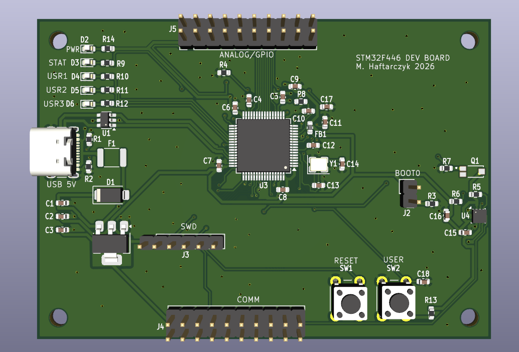
Top layer:
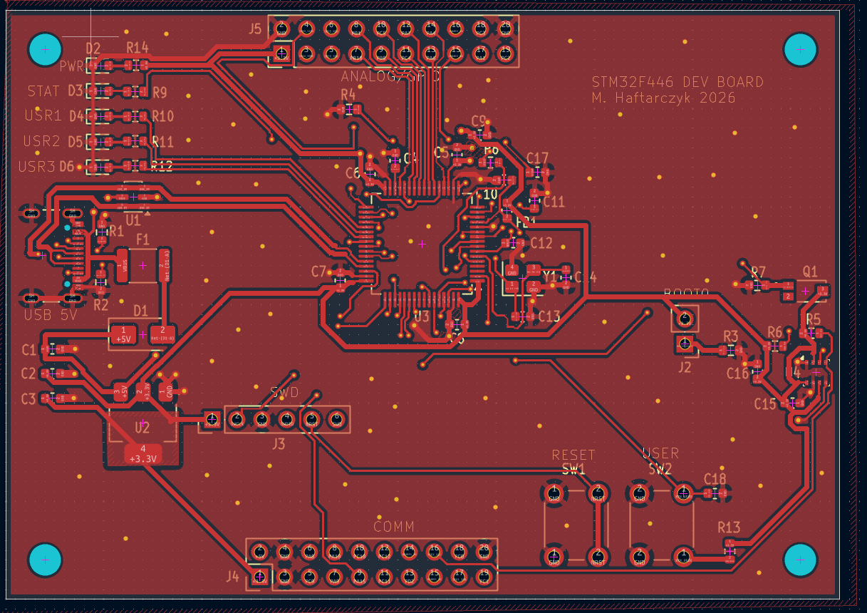
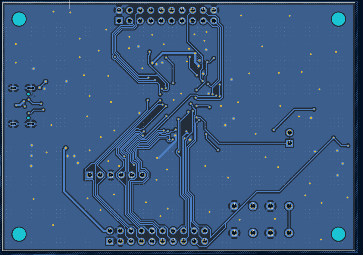
Bottom layer:
Schematic: plytkamh.pdf
The board is 85 x 60 mm, 2 layers, with GND pours on both sides.
SWD (J3):
1  3V3
2  SWCLK (PA14)
3  GND
4  SWDIO (PA13)
5  NRST
6  SWO   (PB3)
COMM (J4):
 1  +3.3V              2  +5V
 3  GND                4  GND
 5  PC9                6  PA8
 7  PA9                8  PA10
 9  PA15              10  PC10
11  PC11              12  PC12
13  PD2               14  USART1_TX (PB6)
15  USART1_RX (PB7)   16  I2C1_SCL  (PB8)
17  I2C1_SDA  (PB9)   18  PC0
19  PC1               20  GND
ANALOG/GPIO (J5):
 1  +3.3V              2  GND
 3  SPI2_MOSI (PB15)   4  SPI2_MISO (PB14)
 5  SPI2_SCK  (PB13)   6  SPI2_NSS  (PB12)
 7  PB10               8  PB1
 9  PB0               10  PC5
11  PC4               12  PA7
13  PA6               14  PA4
15  USART2_RX (PA3)   16  USART2_TX (PA2)
17  PA1               18  PC3
19  PC2               20  GND
On-board stuff: BME280 on PB8/PB9, light sensor on PA0, status LED on PA5, user LEDs on PC6/PC7/PC8, user button on PC13.
USART1 is on PB6/PB7, not on the default PA9/PA10, so it has to be set that way in CubeMX.
plytkamh/
├── plytkamh.kicad_pro
├── plytkamh.kicad_sch
├── plytkamh.kicad_pcb
├── lib/        custom symbols/footprints (LDL1117, TEMT6000)
└── gerber/ files for the PCB manufacturerThe first version of the board was 70 x 50 mm, but I couldn't fit all the header signals, so I made it bigger (85 x 60 mm).
At first the header pinout was done only in the schematic, without thinking about where the pins are on the MCU. During routing it turned out that half of the signals had to go around or under the whole chip. I changed the pinout so J4 gets the pins from the bottom side of the MCU and J5 from the top side, in the same order as on the package. After that the routing was much easier.
Power, USB, the crystal and all the decoupling capacitors were routed by hand. The rest of the GPIO lines going to the headers were routed with Freerouting and then cleaned up manually.
I also had a mistake in the schematic where the crystal wire was shorting PH1 with a few other pins. ERC didn't catch it because it was just one valid net, I found it when checking the netlist.
The BME280 is placed at the edge of the board, far from the LDO and the MCU, so it doesn't measure the heat from the board instead of the air.
Schematic and PCB are done, DRC is clean and the Gerber files are generated. The board hasn't been ordered or tested yet.
| Qty | Value | Footprint | References |
|---|---|---|---|
| 10 | 100n | Capacitor_SMD:C_0603_1608Metric | C3, C5, C6, C7, C8, C11, C12, C15, C16, C18 |
| 4 | 10k | Resistor_SMD:R_0603_1608Metric | R3, R4, R8, R13 |
| 4 | 4.7u | Capacitor_SMD:C_0603_1608Metric | C1, C2, C4, C9 |
| 4 | 680 | Resistor_SMD:R_0603_1608Metric | R9, R10, R11, R12 |
| 4 | MountingHole | MountingHole:MountingHole_3.2mm_M3 | H1, H2, H3, H4 |
| 3 | Red | LED_SMD:LED_0603_1608Metric | D4, D5, D6 |
| 2 | 10p | Capacitor_SMD:C_0603_1608Metric | C13, C14 |
| 2 | 1u | Capacitor_SMD:C_0603_1608Metric | C10, C17 |
| 2 | 4.7k | Resistor_SMD:R_0603_1608Metric | R5, R6 |
| 2 | 5.1k | Resistor_SMD:R_0603_1608Metric | R1, R2 |
| 1 | 0.5A | Fuse:Fuse_1812_4532Metric | F1 |
| 1 | 12MHz | Crystal:Crystal_SMD_3225-4Pin_3.2x2.5mm | Y1 |
| 1 | 3.3k | Resistor_SMD:R_0603_1608Metric | R7 |
| 1 | 470 | Resistor_SMD:R_0603_1608Metric | R14 |
| 1 | 600R@100MHz | Inductor_SMD:L_0603_1608Metric | FB1 |
| 1 | ANALOG_GPIO | Connector_PinHeader_2.54mm:PinHeader_2x10_P2.54mm_Vertical | J5 |
| 1 | BME280 | Package_LGA:Bosch_LGA-8_2.5x2.5mm_P0.65mm_ClockwisePinNumbering | U4 |
| 1 | BOOT0 | Connector_PinHeader_2.54mm:PinHeader_1x02_P2.54mm_Vertical | J2 |
| 1 | COMM | Connector_PinHeader_2.54mm:PinHeader_2x10_P2.54mm_Vertical | J4 |
| 1 | Conn_01x06 | Connector_PinHeader_2.54mm:PinHeader_1x06_P2.54mm_Vertical | J3 |
| 1 | Green | LED_SMD:LED_0603_1608Metric | D2 |
| 1 | LDL1117S33R | Package_TO_SOT_SMD:SOT-223 | U2 |
| 1 | RESET | Button_Switch_THT:SW_PUSH_6mm | SW1 |
| 1 | SS14 | Diode_SMD:D_SMA | D1 |
| 1 | STM32F446RETx | Package_QFP:LQFP-64_10x10mm_P0.5mm | U3 |
| 1 | TEMT6000X01 | TEMT6000X01:TRANS_TEMT6000X01 | Q1 |
| 1 | USBLC6-2SC6 | Package_TO_SOT_SMD:SOT-23-6 | U1 |
| 1 | USB_C_Receptacle_USB2.0_16P | Connector_USB:USB_C_Receptacle_GCT_USB4105-xx-A_16P_TopMnt_Horizontal | J1 |
| 1 | USER | Button_Switch_THT:SW_PUSH_6mm | SW2 |
| 1 | Yellow | LED_SMD:LED_0603_1608Metric | D3 |
KirtiChickamath/ESP32-IoT-sensor-board
ESP32- IoT sensor board. 4-layer PCB, designed in KiCad . Features LiPo charging, USB-C, SPI flash, SD card, BME280, and more.


Ankithkumarsingh/ESP32-custom-sensor-board
This PCB contains the power supply unit, ESP32 module as compute, microphone sensor, light sensing sensor, SDCard module for data logging.

aryan-asit/Telemetry-iot-project
In this project , a 4 layer custom pcb is made for Telematics

ddennis18/ESP32-IoT-DevBoard
An ESP32-C3 based IoT controller board designed in KiCad. The board combines wireless control, sensor interfaces, local storage, audio/light sensing, USB connectivity, and single-cell Li-ion battery support on a compact…

EngMeesh/ESP32_IoT_Dev_Board
A custom 4-layer IoT development board based on the ESP32-C3, featuring integrated LiPo battery management, a CP2102N USB-UART bridge, MicroSD support, and onboard environmental/audio sensors for embedded engineering…

kaushal1020/esp32-c3-02-KiCAD-Design
A custom ESP32-C3-02 Development Board designed from scratch using KiCad. This repository contains the complete hardware design, including schematic, PCB layout, and supporting files for manufacturing and development.

pravinsharma15k-ops/ESP32-C3-Sensor-Board
Battery-powered ESP32-C3 sensor board with USB-C charging, KiCad 10 design files
It measures 85 × 60 mm and has 2 copper layers, 1.6 mm thick.
57 parts, built around the BME280, TEMT6000X01, LDL1117S33R and USBLC6-2SC6. The full list of its parts is on this page, with links to each part's symbol and footprint where PCBKit's library has them.
From the mhaftarc/pcb_project_mh repository on GitHub, at the commit this page was made from: the board is plytkamh/plytkamh.kicad_pcb and its schematic plytkamh/plytkamh.kicad_sch. PCBKit opens the board in the browser, with nothing to install.
Its repository states no licence, so its author keeps all rights: ask mhaftarc before reusing the design.