
4 layers174 × 104 mm

 mengstr/DCJ11_carrier1
A carrier PCB for the DEC DCJ11 CPU
DCJ11 carrier is an open-source printed circuit board by mengstr, from the mengstr/DCJ11_carrier repository on GitHub, published under the MIT licence. It is a 2-layer board of 35.6 × 77.5 mm with 29 parts on 61 nets, routed with 158 tracks and 5 vias.
It is built around the B220. Its parts include 19 resistors, 4 diodes, 4 connectors and 2 capacitors.
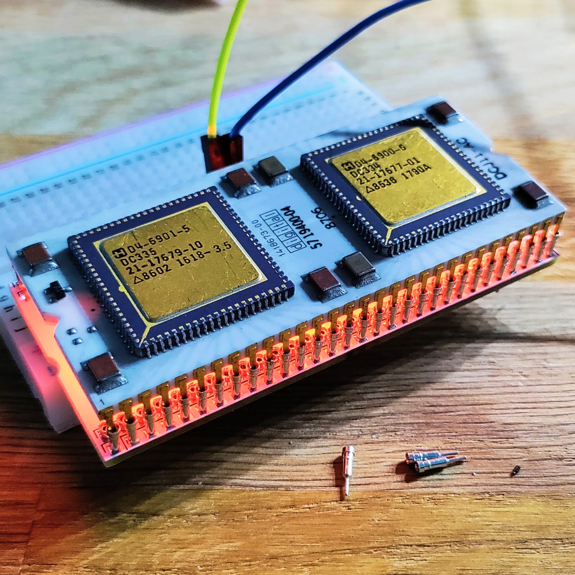
To protect the sensitive pins on the DCJ11 CPU, I designed a small carrier board to keep it safe.
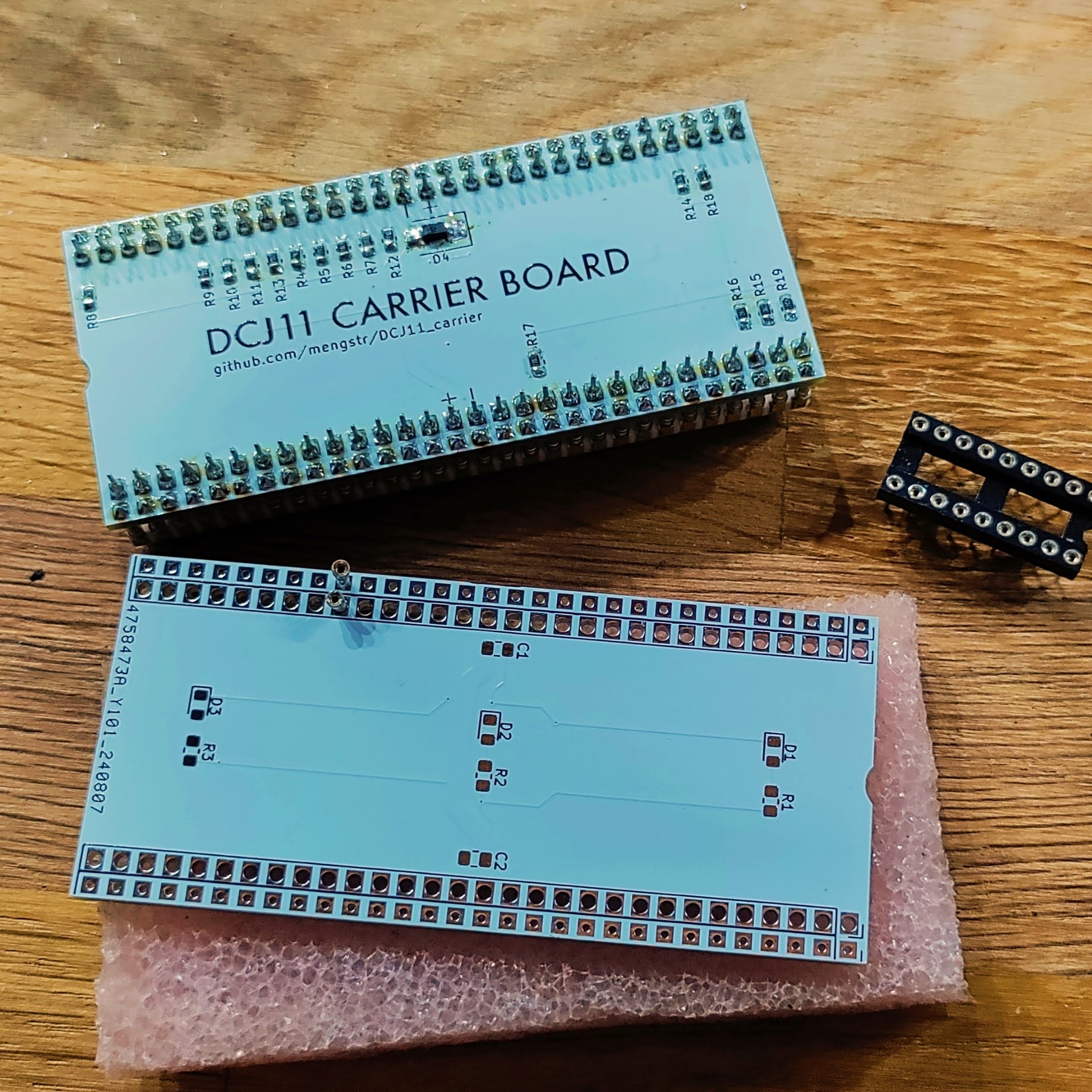
I added a few extras to the board, like reverse polarity protection—just a simple reverse diode that shorts the power if applied incorrectly. (I know it really should have been a proper P-MOS instead, but hey, it’s better than nothing.)
I also included pull-ups and pull-downs on the inputs since many of them won’t be in use for simple applications. This keeps them stable at the carrier level, so there’s no need to add jumpers externally. After the images here is a table with the pinout indicating which pins that have the pulls on them.
There are also two extra capacitor footprints on the top side of the carrier if needed, though the DCJ11 itself seems to have plenty of local capacitance. Just for fun, I added footprints for a few LEDs and resistors, hoping that the ceramic package of the DCJ11 would let some light through and create a cool glowing effect—but no joy. The ceramic is completely opaque.
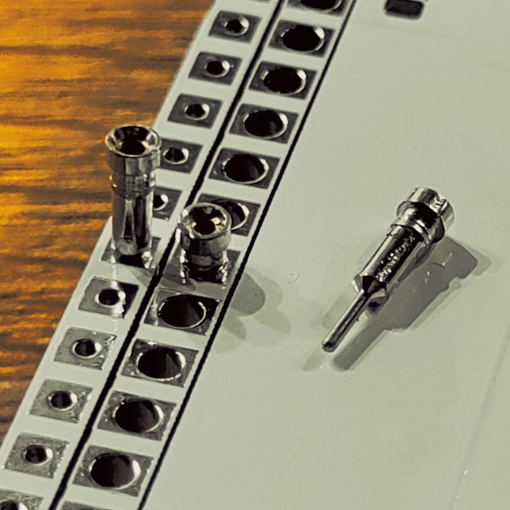
The PCB is designed to use turned IC socket contacts. The row with smaller holes is for the DCJ11 itself, lifting it up a few millimeters above the PCB. The larger holes allow the contacts to drop down fully to their flanges, making them protrude as much as possible below the board so the carrier can later be inserted into the user motherboard.
| Pin# | Direction | Pull | Name | Description |
|---|---|---|---|---|
| 1 | in | pu | nTEST1 | Test input |
| 2 | out | AIO 0 | Address I/O 0 | |
| 3 | out | AIO 1 | Address I/O 1 | |
| 4 | out | AIO 2 | Address I/O 2 | |
| 5 | out | AIO 3 | Address I/O 3 | |
| 6 | in | pu | nPWRF | Power fail |
| 7 | in | pu | nFPE | Floating-point error |
| 8 | in | pu | nEVENT | Event interrupt |
| 9 | in | pd | HALT | Halt processor |
| 10 | in | pd | IRQ0 | Interrupt request 0 |
| 11 | in | pd | IRQ1 | Interrupt request 1 |
| 12 | in | pd | IRQ2 | Interrupt request 2 |
| 13 | in | pd | IRQ3 | Interrupt request 3 |
| 14 | in | pu | nPARITY | Parity check |
| 15 | - | GND | Ground (0V) | |
| 16 | - | VCC | Power (5V) | |
| 17 | out | BS 0 | Bus strobe 0 | |
| 18 | out | BS 1 | Bus strobe 1 | |
| 19 | out | nMAP | Memory map control | |
| 20 | i/o | nABORT | Abort cycle | |
| 21 | out | DAL21 | Data/address line 21 | |
| 22 | out | DAL20 | Data/address line 20 | |
| 23 | out | DAL19 | Data/address line 19 | |
| 24 | out | DAL18 | Data/address line 18 | |
| 25 | out | DAL17 | Data/address line 17 | |
| 26 | out | DAL16 | Data/address line 16 | |
| 27 | in | pu | nDMR | DMA request |
| 28 | in | pu | nMISS | Cache miss |
| 29 | out | nPRDC | Predict control | |
| 30 | - | N.C. | Unused pin | |
| 31 | in | pu | nTEST2 | Test output |
| 32 | in | pu | nCONT | Continue signal |
| 33 | in | pu | nINIT | Initialize |
| 34 | out | CLK2 | Clock 2 | |
| 35 | i/o | CLK | Clock | |
| 36 | in | XTALHI | Crystal input | |
| 37 | out | XTALLO | Crystal output | |
| 38 | out | nSCTL | Strobe control | |
| 39 | out | nSTRB | Strobe signal | |
| 40 | out | nALE | Address latch enable | |
| 41 | out | nBUFCTL | Buffer control | |
| 42 | in | pu | DV | Device vector |
| 43 | i/o | DAL5 | Data/address line 5 | |
| 44 | i/o | DAL4 | Data/address line 4 | |
| 45 | - | GND | Ground (0V) | |
| 46 | - | VCC | Power (5V) | |
| 47 | i/o | DAL3 | Data/address line 3 | |
| 48 | i/o | DAL2 | Data/address line 2 | |
| 49 | i/o | DAL1 | Data/address line 1 | |
| 50 | i/o | DAL15 | Data/address line 15 | |
| 51 | i/o | DAL14 | Data/address line 14 | |
| 52 | i/o | DAL13 | Data/address line 13 | |
| 53 | i/o | DAL12 | Data/address line 12 | |
| 54 | i/o | DAL11 | Data/address line 11 | |
| 55 | i/o | DAL10 | Data/address line 10 | |
| 56 | i/o | DAL9 | Data/address line 9 | |
| 57 | i/o | DAL0 | Data/address line 0 | |
| 58 | i/o | DAL8 | Data/address line 8 | |
| 59 | i/o | DAL7 | Data/address line 7 | |
| 60 | i/o | DAL6 | Data/address line 6 |
| Qty | Value | Footprint | References |
|---|---|---|---|
| 19 | R | Resistor_SMD:R_0805_2012Metric_Pad1.20x1.40mm_HandSolder | R1, R2, R3, R4, R5, R6, R10, R11, R12, R13, R14, R15, R16, R17, R18, R19 +3 |
| 4 | Conn_01x30_Socket | Connector_PinSocket_2.54mm:PinSocket_1x30_P2.54mm_Vertical | J1, J2, J3, J4 |
| 3 | LED | LED_SMD:LED_0805_2012Metric_Pad1.15x1.40mm_HandSolder | D1, D2, D3 |
| 2 | C | Capacitor_SMD:C_0805_2012Metric_Pad1.18x1.45mm_HandSolder | C1, C2 |
| 1 | B220 | Diode_SMD:D_SMB | D4 |


manhoosbilli1/atmega328-enclosure-tamper-alarm
ATmega328 AC enclosure tamper/intrusion alarm with LTC2960 voltage monitor, LTC4412 PowerPath, boost+buck converters

ManuelArgibay/BLDC-ESC-PCB
PCB de 4 capas en KiCad para un ESC sensorless de motor BLDC (IR2301 + LM339, detección de BEMF) con Tiva C TM4C123GXL

Miguel-Barcelos/Electronics-Projects
Este repositório contém projetos de eletrônica, incluindo circuitos eletrônicos, simulações e design de PCBs.

rohamid/Nextion_USB_serial_downloader
A PCB for powering and downloading Nextion HMI directly using USB to Serial

It measures 35.6 × 77.5 mm and has 2 copper layers, 1.6 mm thick.
29 parts, built around the B220. The full list of its parts is on this page, with links to each part's symbol and footprint where PCBKit's library has them.
From the mengstr/DCJ11_carrier repository on GitHub, at the commit this page was made from: the board is DCJ11_Carrier/DCJ11_Carrier.kicad_pcb and its schematic DCJ11_Carrier/DCJ11_Carrier.kicad_sch. PCBKit opens the board in the browser, with nothing to install.
Its repository publishes it under the MIT licence: you may reuse it on that licence's terms (keep the author's notice, and for a copyleft licence share your changes alike).