2 layers43.9 × 27.7 mm
 MeBadDev/HackPad
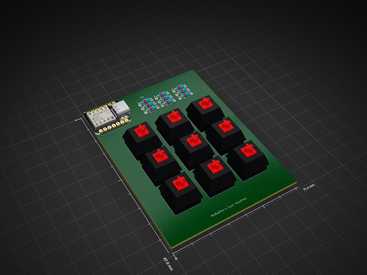
HackPad is an open-source printed circuit board by MeBadDev, from the MeBadDev/HackPad repository on GitHub. It is a 2-layer board of 71.4 × 97.6 mm with 19 parts on 23 nets, routed with 95 tracks and 9 vias.
Its parts include 9 diodes, 9 switches and 1 IC. It belongs with the RP2040 boards of this library.
This is my submission to HackClub HackPad v4! It's also my first ever hardware project.
I originally wanted to build a 80% keyboard, but don't know anything about electronics. I found some tutorials and dumbed it down into something I can manage, fits in HackPad's requirement, and still helps me learn to build a keyboard (I've learnt how matrixes work, for example)!
I've learnt quite a bit about electronics and (probably, when i got my hands on the hardware) soldering. I've also learnt about the general process of designing a PCB, and how to use KiCad. It's been a fun experience so far!
The HackPad guide is really good, and I highly recommend it to anyone wanting to get into hardware! I've also fixed some typos and mistakes in the guide, so check that out if you're interested!
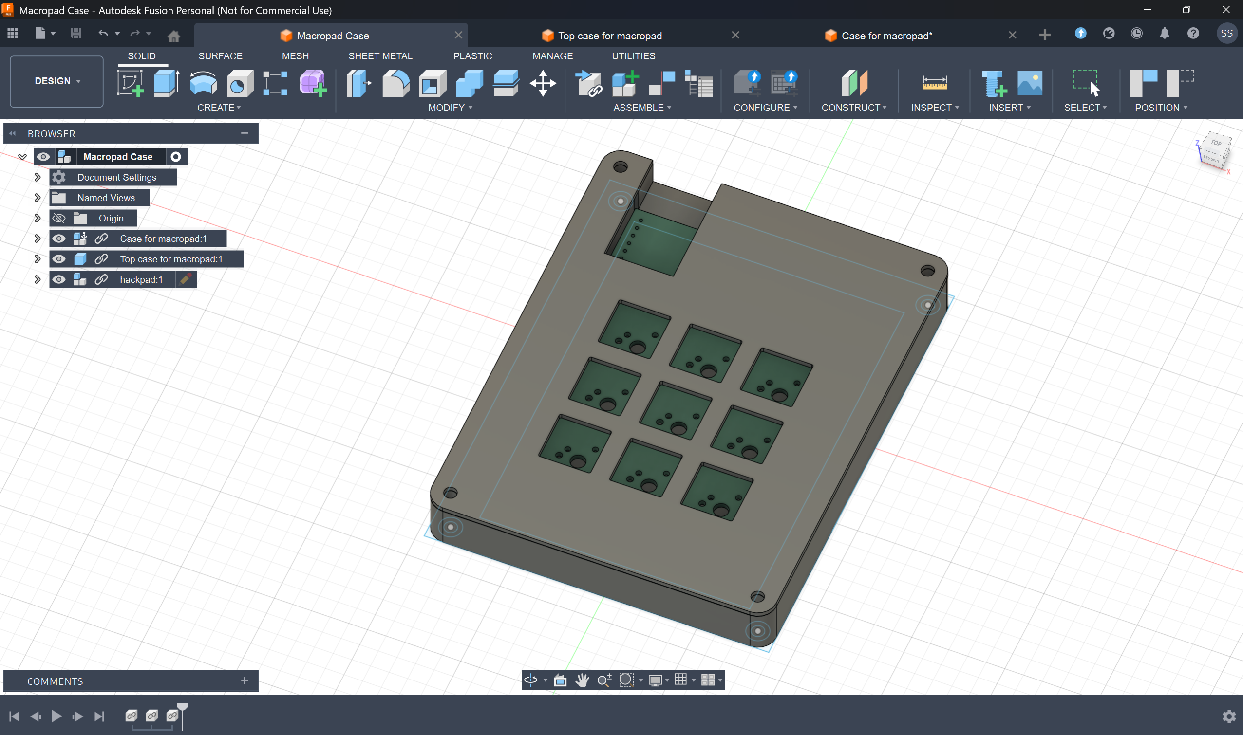
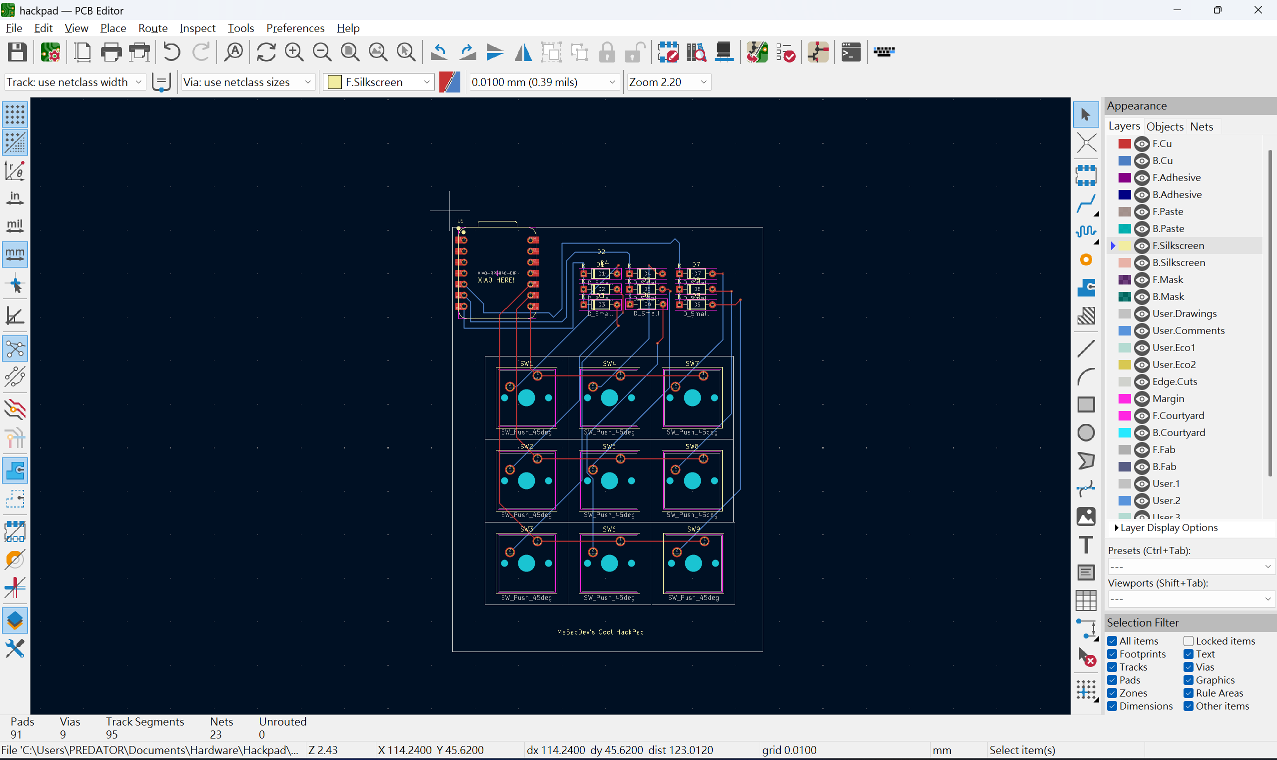
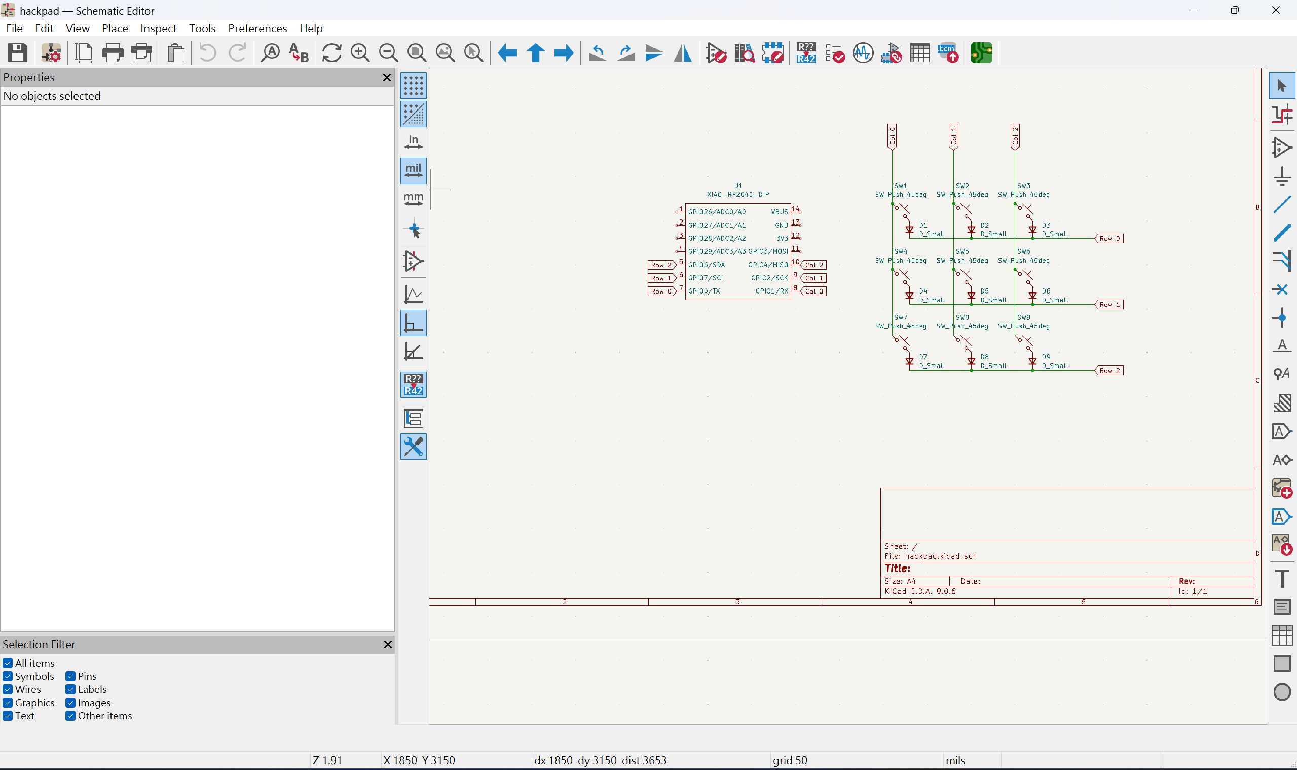
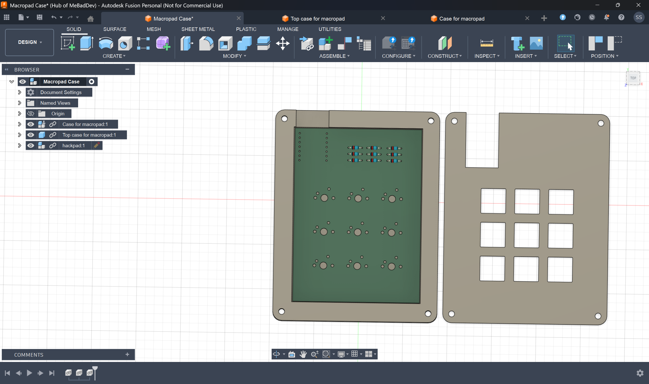
I'll update this README when I make more progress on the project, and perhaps write a blog post about it too! See you!
| Qty | Value | Footprint | References |
|---|---|---|---|
| 9 | D_Small | Diode_THT:D_DO-35_SOD27_P7.62mm_Horizontal | D1, D2, D3, D4, D5, D6, D7, D8, D9 |
| 9 | SW_Push_45deg | Button_Switch_Keyboard:SW_Cherry_MX_1.00u_PCB | SW1, SW2, SW3, SW4, SW5, SW6, SW7, SW8, SW9 |
| 1 | XIAO-RP2040-DIP | OPL:XIAO-RP2040-DIP | U1 |
It measures 71.4 × 97.6 mm and has 2 copper layers, 1.6 mm thick.
19 parts. The full list of its parts is on this page, with links to each part's symbol and footprint where PCBKit's library has them.
From the MeBadDev/HackPad repository on GitHub, at the commit this page was made from: the board is PCB/hackpad.kicad_pcb and its schematic PCB/hackpad.kicad_sch. PCBKit opens the board in the browser, with nothing to install.
Its repository states no licence, so its author keeps all rights: ask MeBadDev before reusing the design.

hackclub/OnBoard
💡 Join 1,000 teenagers and make your first PCB with a $100 grant!

polpo/picogus
Emulation of ISA sound cards and CD-ROM on Raspberry Pi Pico (GUS, SB/Adlib, MPU-401, Tandy, CMS, Panasonic CD-ROM) with USB mouse/joystick support


nkitanov/iaq_board
IAQ Board is a DIY (Do-It-Yourself) device for measuring internal air quality


Ardumower/ardumower
Develop an open source robotic lawn mower (HW+SW reference platform)

zmaker/arduino_cookbook
gli sketch del nuovo progetto Arduino Cookbook e dei video di YouTube