

4 layers48.3 × 24.1 mm

 mct814/Pipe-Mapping-Project2
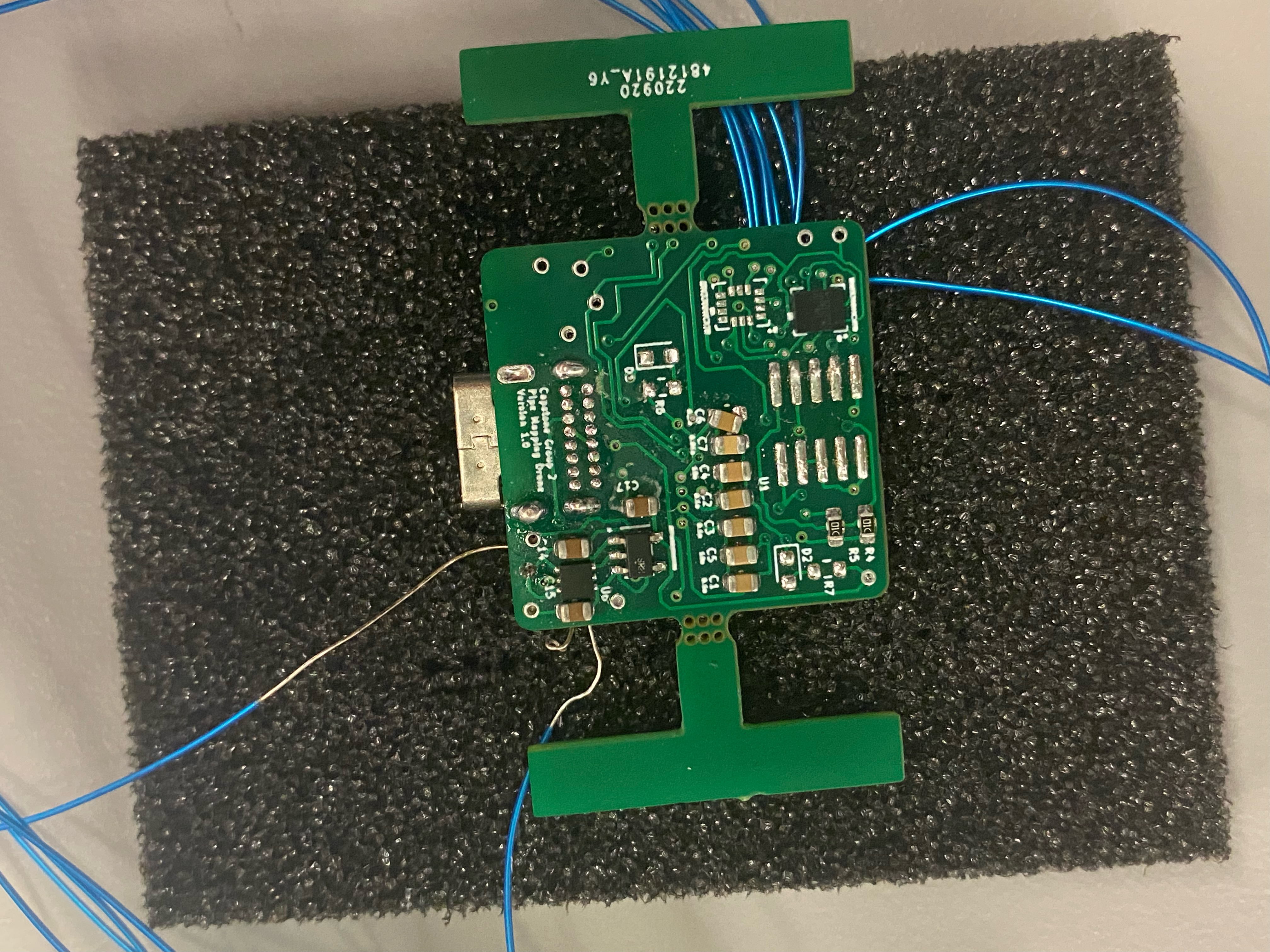
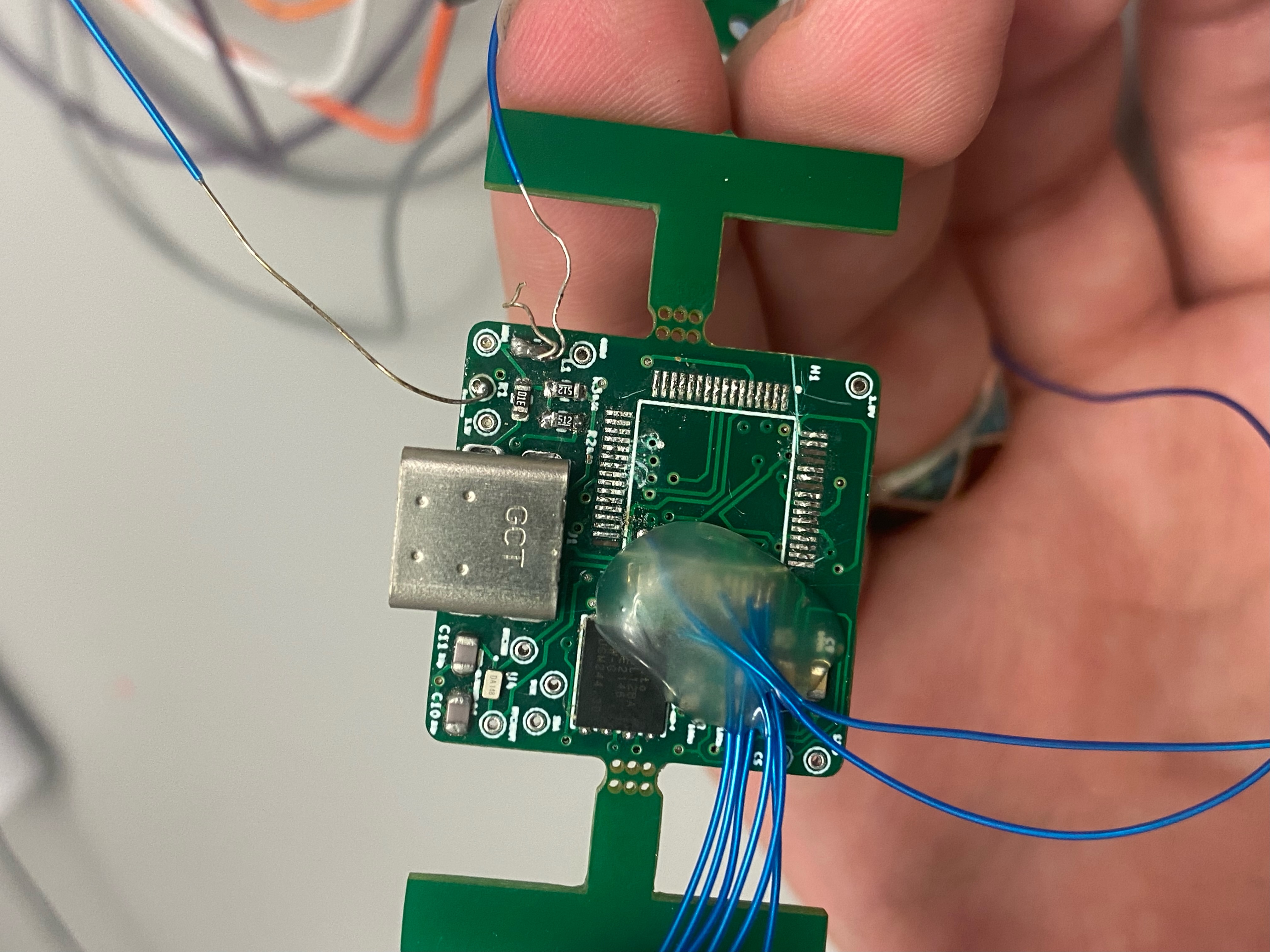
Capstone V2 is an open-source printed circuit board by mct814, from the mct814/Pipe-Mapping-Project repository on GitHub, published under the MIT licence. It is a 2-layer board of 43.2 × 17.8 mm with 21 parts on 39 nets, routed with 208 tracks and 27 vias.
It is built around the AT25SL128A-MHE-T and ISM330DHCXTR.
The problem that we wish to solve is a simple one. Underground PVC piping is often necessary to fix but difficult to locate. Methods currently exist for the detection of large industrial pipes, but there is a distinct lack of such technology for small, residential PVC pipes. This project proposes a new way of mapping pipe networks by using a small probe to record positional data while harmlessly traversing the pipe. The team’s objective is to create a probe based system to traverse and map variable sized underground pipe networks in 3D space, within an acceptable margin of error. While developing a mechanical pipe traversal method for the probe is part of this project, the primary goal consists of setting up the base technology for 3D mapping and real time information collection inside of 2"-4" PVC pipe.
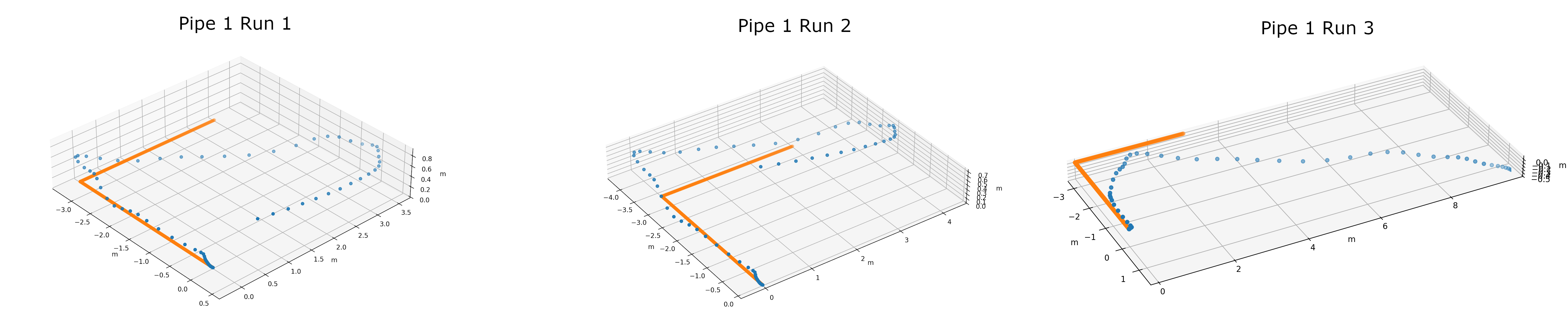
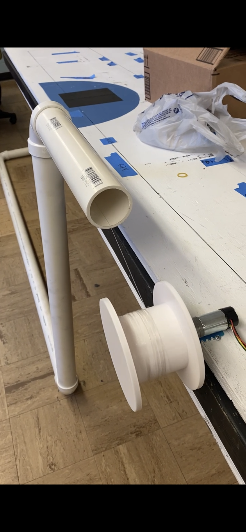
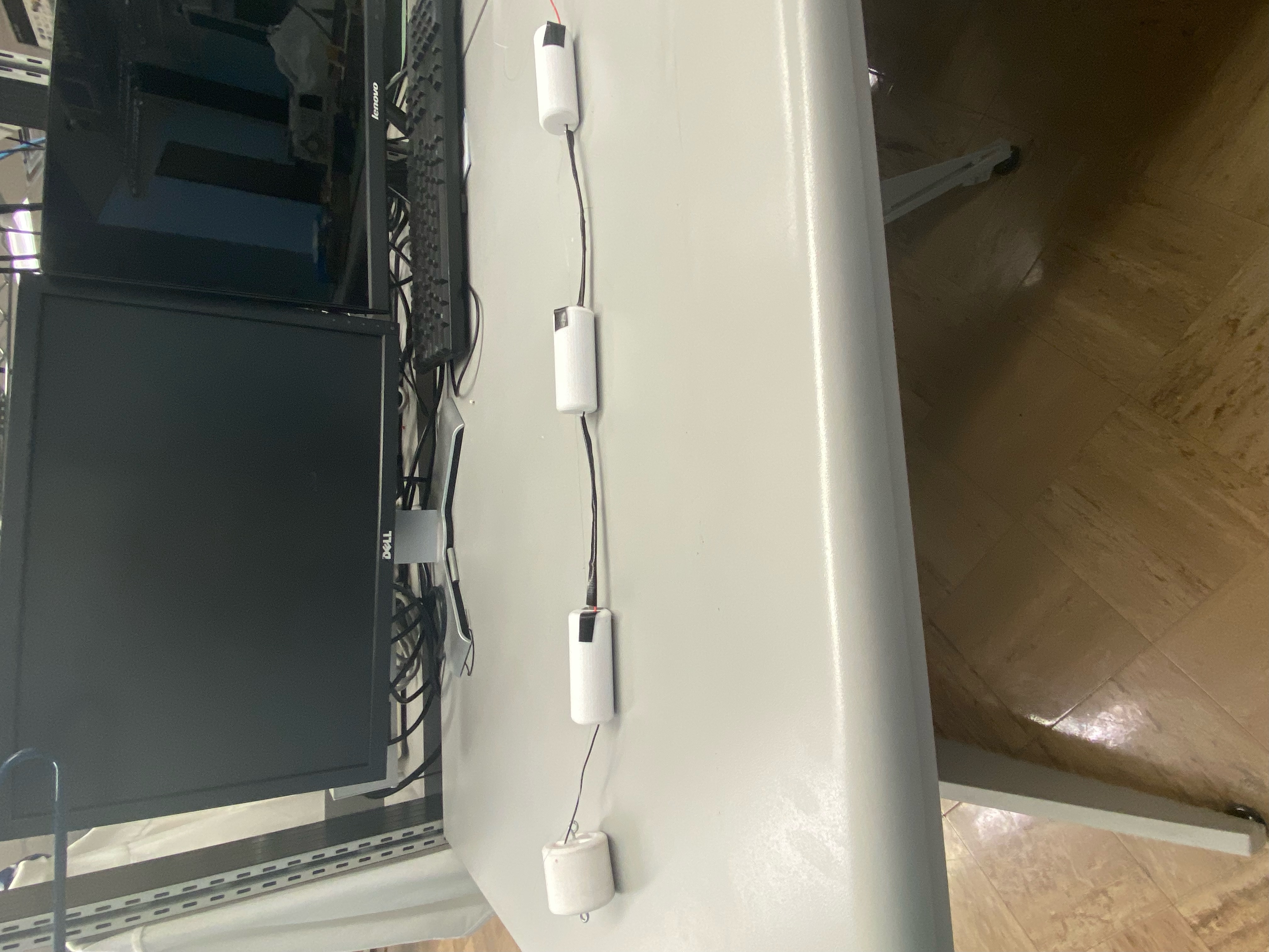
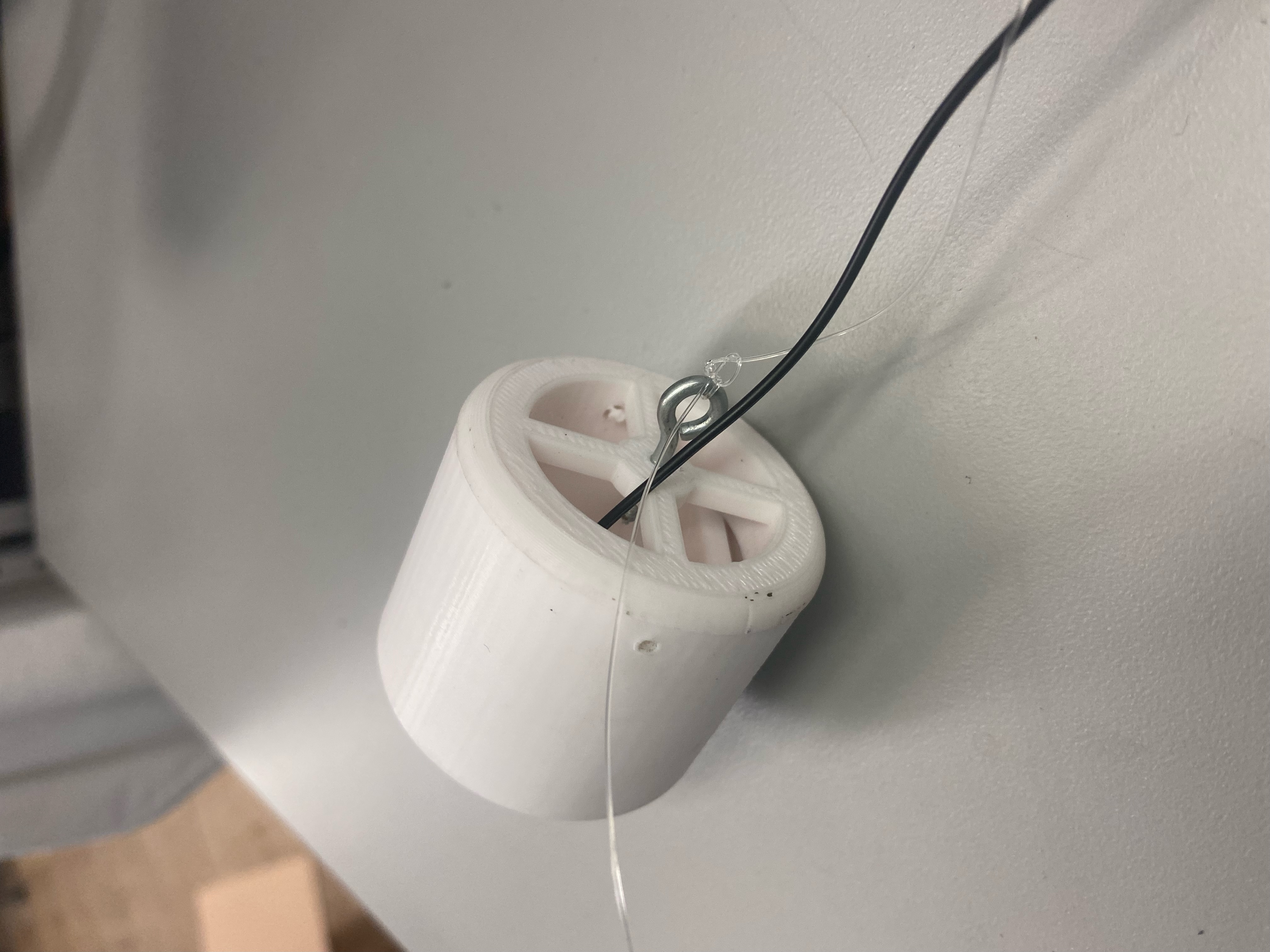
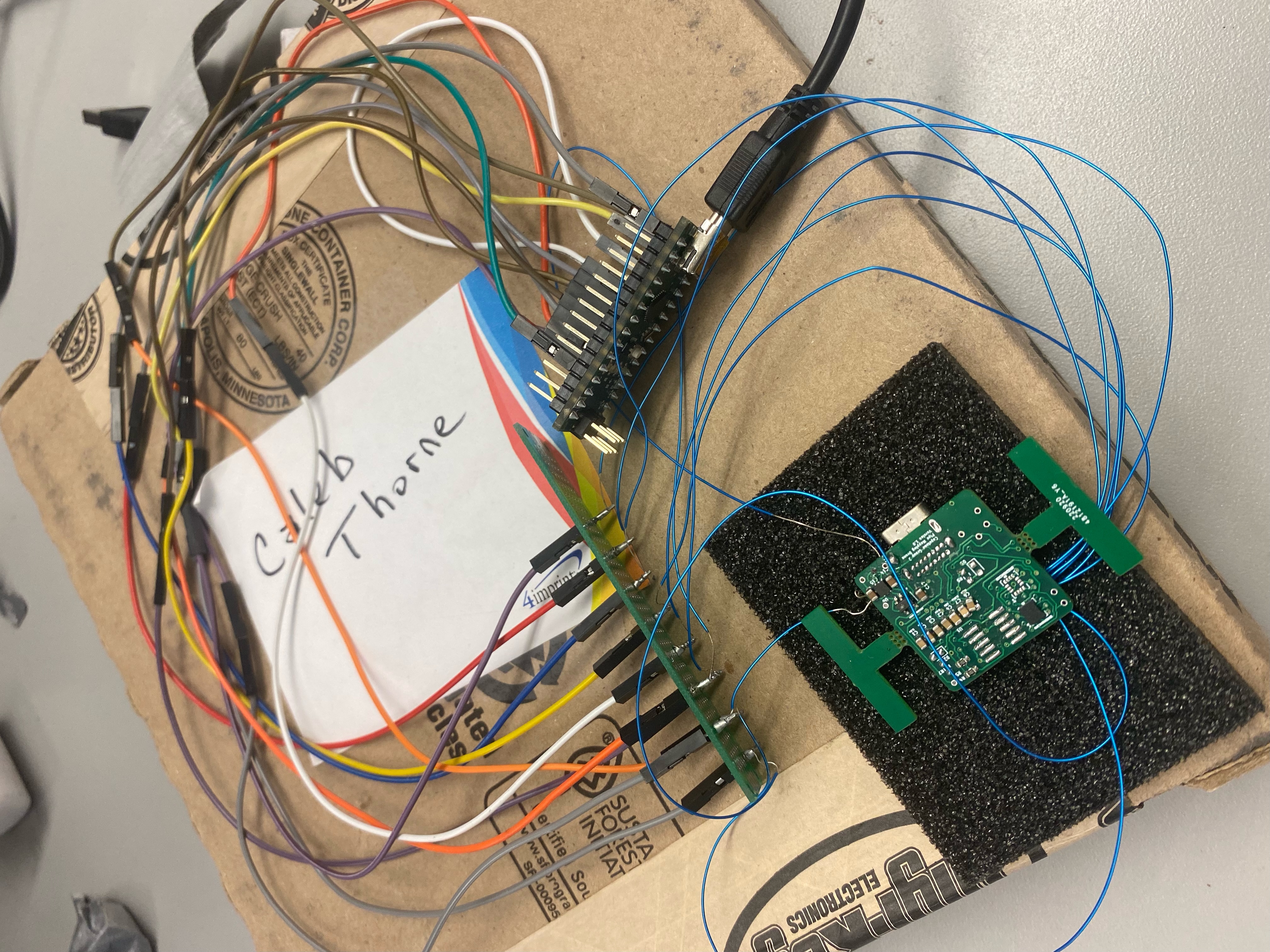
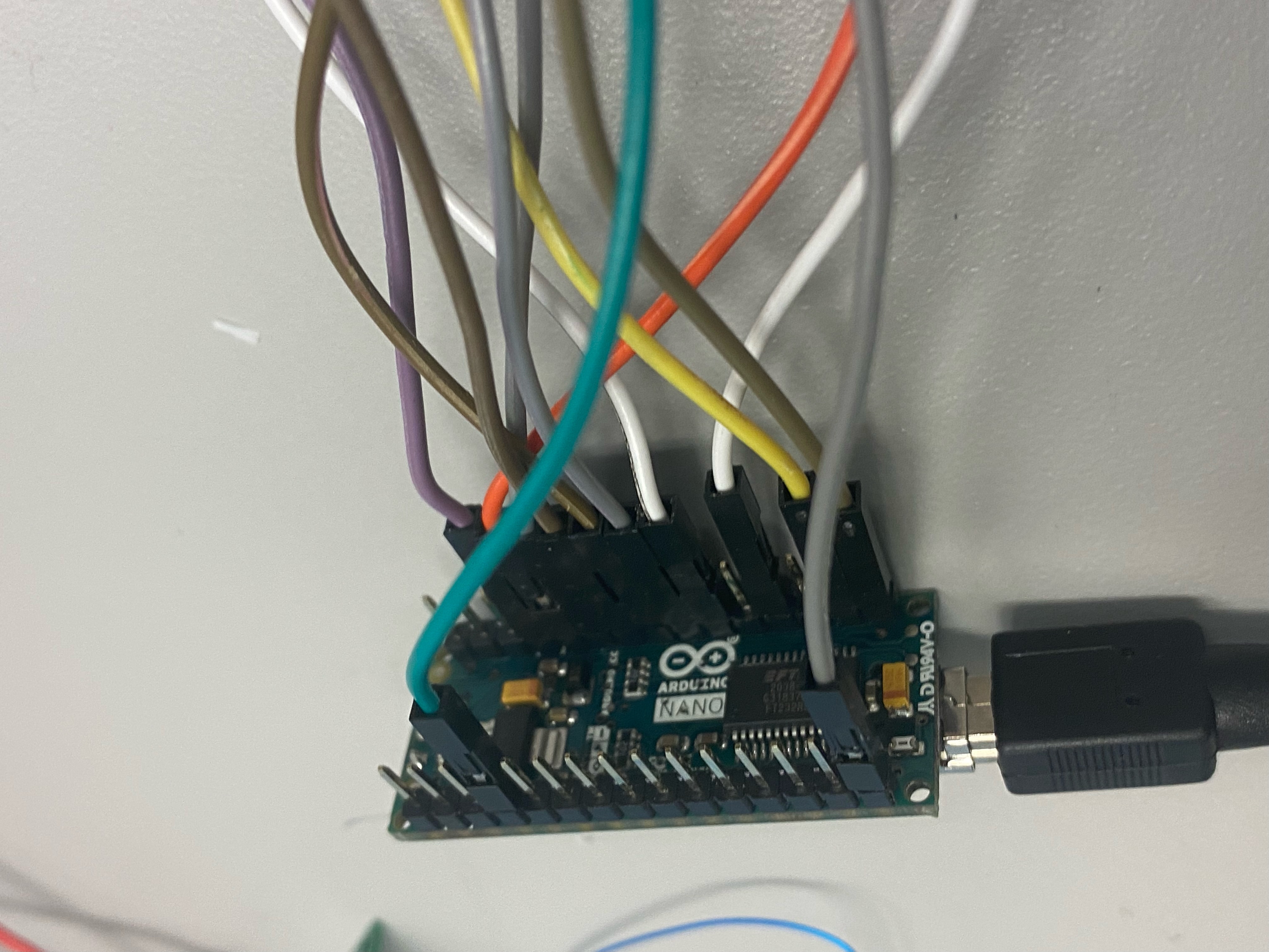
The current version of our design is still in the testing phase. While we have developed a functional testing system including a probe casing, pulley system and PVC network our current probe cannot fit inside the PVC pipe. The probe is using an arduino nano to pole data points and connect to the laptop which runs the mapping software. This probe can collect data while being powered by a set of 3 AA batteries and transmit said data to the PC. We have designed an improved system that would fit inside the 2" pipe but we have not yet implemented it. Our current mapping software can get data points within a relativiely similar shape to the physical path but still has a large margin of error. Further develpment of the mapping software is required to get within our original specification of 1" margin of error.
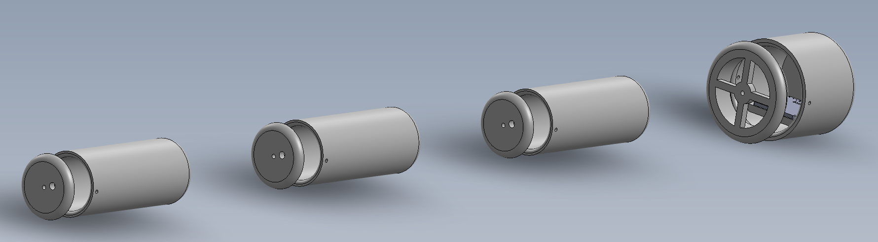
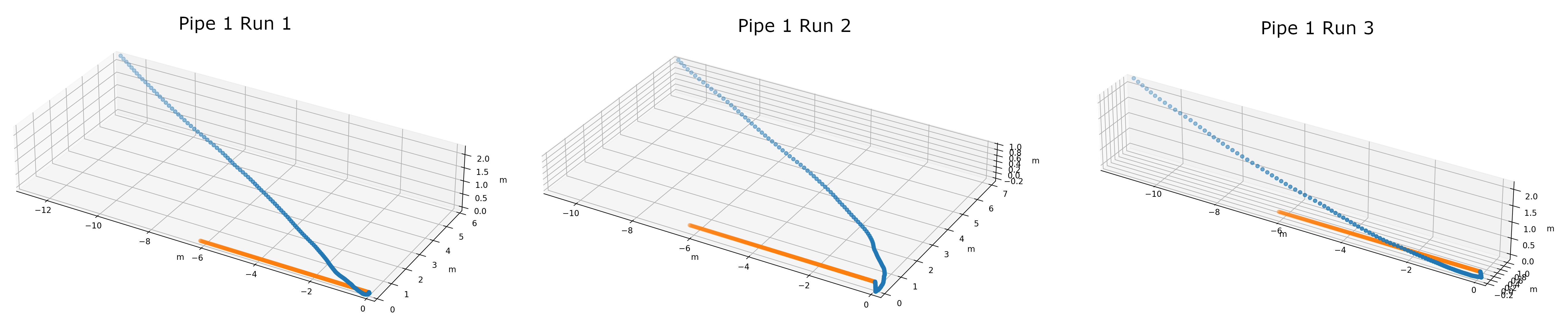
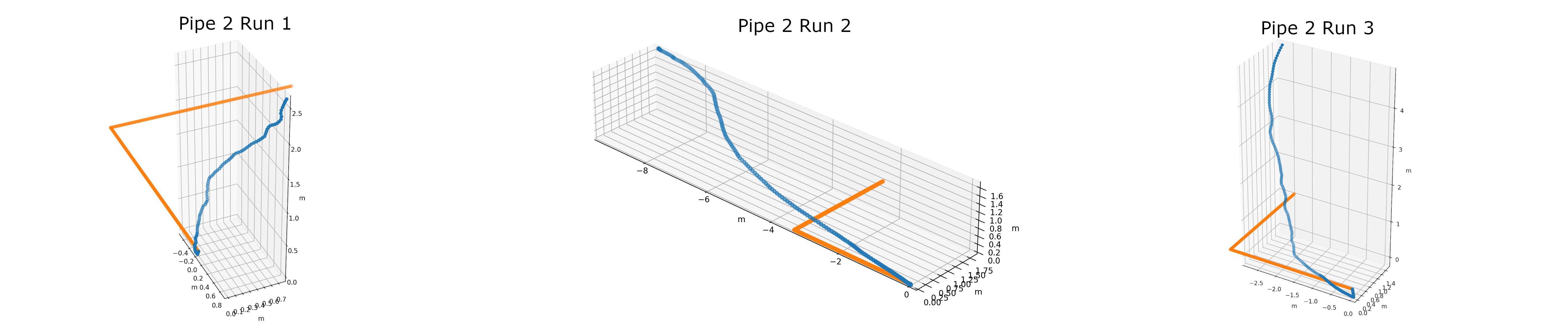
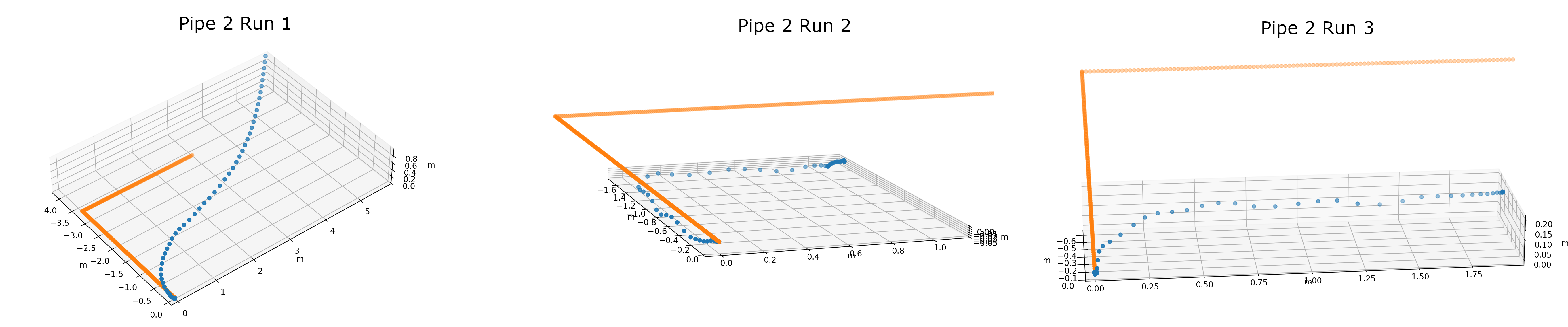
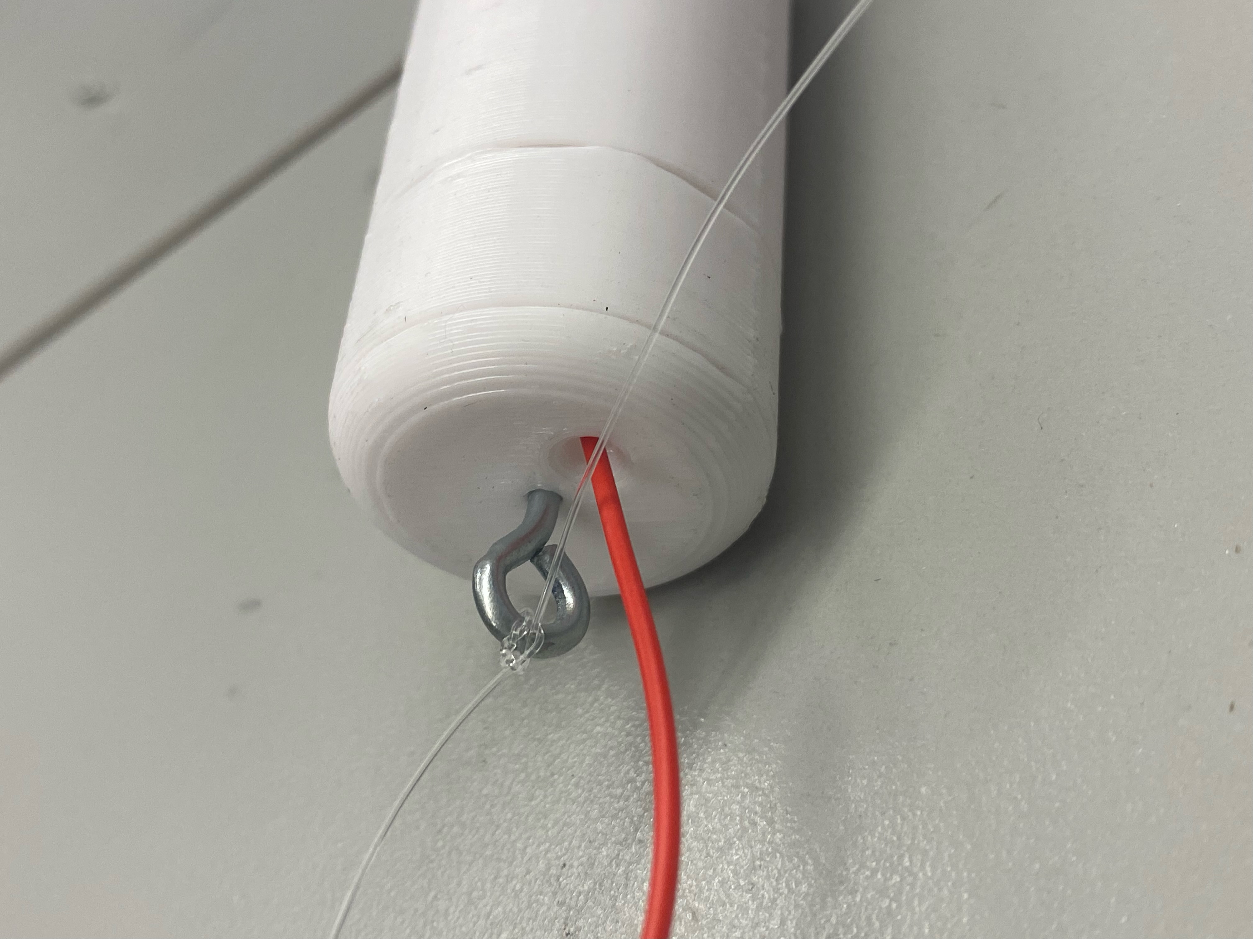
Our main successes came in the form of the mechanical testing system shown below and the preliminary maps created during testing.
I am a computer engineering senior at Tennessee Technological University. I am originally from Knoxville, TN and graduated from Bearden High School.
I am a computer engineering senior at Tennessee Technological University. I am originally from Greensboro, NC and graduated from Ravenwood High School.
I am an electrical engineering senior at Tennessee Technological University. I am originally from Pulaski, TN and graduated from Giles County High School.
I am an electrical engineering senior at Tennessee Technological University. I am originally from Tullahoma, TN and graduated from Family Christian Academy.
The main file of the repository contains the lisence, readme, planned software file, reports folder, and project documentation folder. Inside of the reports folder are the original project proposal, the design phase 1 document, and the final report. Inside the project documentation folder is the bill of materials, project schematic and the folders for each of the subsystems that have been designed. Each of the subsystem folders contains schematics and readme descriptions of the design process.
| Qty | Value | Footprint | References |
|---|---|---|---|
| 4 | 100n | Capacitor_SMD:C_0603_1608Metric_Pad1.08x0.95mm_HandSolder | 100n, 100n, 100n, 100n |
| 4 | MountingHole | MountingHole:MountingHole_2.1mm | H1, H2, H3, H4 |
| 3 | 1u | Capacitor_SMD:C_0603_1608Metric_Pad1.08x0.95mm_HandSolder | 1u, 1u, 1u |
| 2 | Conn_01x15 | Connector_Molex:Molex_KK-254_AE-6410-15A_1x15_P2.54mm_Vertical | J1, J2 |
| 2 | ISM330DHCXTR | IMU:ISM330DHCXTR | IMU1, IMU2 |
| 2 | TestPoint | TestPoint:TestPoint_THTPad_2.5x2.5mm_Drill1.2mm | BATTERY, GND |
| 1 | 2.2u | Capacitor_SMD:C_0603_1608Metric_Pad1.08x0.95mm_HandSolder | 2.2u |
| 1 | AT25SL128A-MHE-T | Memory:AT25SL128A-MHE-T | MEMORY |
| 1 | LD2981ABM50TR | 5LDO:LD2981ABM50TR | 5V LDO |
| 1 | NCP163ASN180T1G | 18LDO:NCP163ASN180T1G | 1.8V LDO |


It measures 43.2 × 17.8 mm and has 2 copper layers, 1.6 mm thick.
21 parts, built around the AT25SL128A-MHE-T and ISM330DHCXTR. The full list of its parts is on this page, with links to each part's symbol and footprint where PCBKit's library has them.
From the mct814/Pipe-Mapping-Project repository on GitHub, at the commit this page was made from: the board is projectDocumentation/redesign/pcbSubsystem/Capstone_V2/Capstone_V2.kicad_pcb and its schematic projectDocumentation/pcbSubsystem/KiCAD_PCB_Design/Capstone.kicad_sch. PCBKit opens the board in the browser, with nothing to install.
Its repository publishes it under the MIT licence: you may reuse it on that licence's terms (keep the author's notice, and for a copyleft licence share your changes alike).