Skip to the content
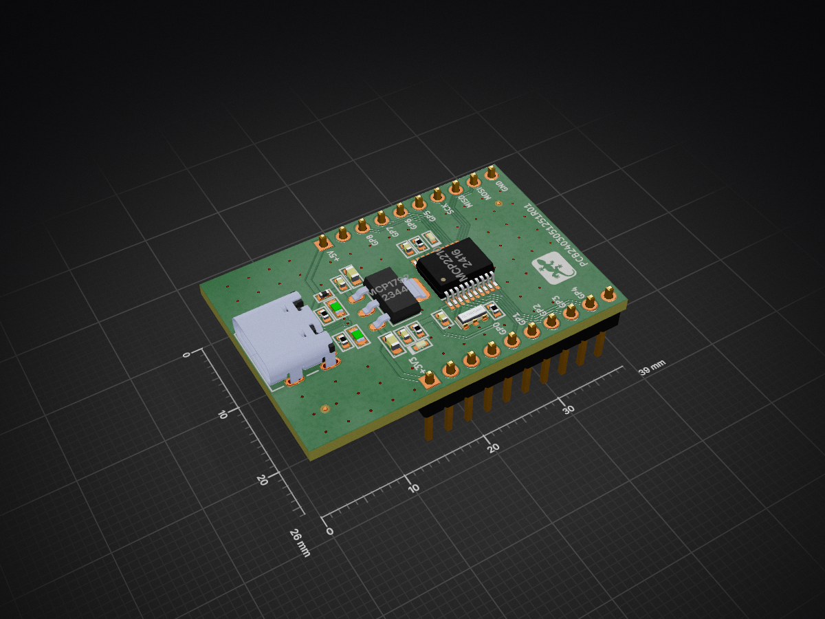
2 layers39 × 26 mmMCP2210 Eval kit, the printed circuit board in 3D

MCP2210 Eval kit

mbeale13/PCB_USBToSpi
Size
39 × 26 mm
Copper layers
2
Thickness
1.6 mm
Parts
25
Nets
31
Pads
99
Tracks, vias
172, 79
Pours
2
Routed
Yes
KiCad
KiCad 9.0 (file 20241229)
Created
11 Oct 2026
Updated
17 Oct 2026

Overview

MCP2210 Eval kit is an open-source printed circuit board by mbeale13, from the mbeale13/PCB_USBToSpi repository on GitHub. It is a 2-layer board of 39 × 26 mm with 25 parts on 31 nets, routed with 172 tracks and 79 vias.

It is built around the MCP2210-I/MQ, PGB1010603MR and LI0402B301R-10, with the USB4105-GF-A among its other parts. Its parts include 6 capacitors, 5 resistors, 4 diodes, 3 connectors and 2 ICs.

Main components

4

Parts

25
QtyValueFootprintReferences
4100nFCapacitor_Library:C_0402C1, C3, C5, C6
23k3Resistor_Library:R_0402R3, R5
24.7uFCapacitor_Library:C_0603C2, C4
2FiducialFiducial:Fiducial_0.5mm_Mask1mmFID1, FID2
2HDR_1X10Connector_Library:HDRSRST10P100MILJ2, J3
2LEDDiode_Library:LED_0402D3, D4
2PGB1010603MRTranzorb_Library:TRANZORB 0603D1, D2
1390RResistor_Library:R_0402R4
15k1My_Resistors:R_0402R1
15k1Resistor_Library:R_0402R2
1CSTNE12M0Timing_Library:CERRESNY1
1Gecko_logoMisc_Library:Gecko_logo 5mm x 7mmGecko1
1LI0402B301R-10Inductor_Library:FERRITE_BEAD_0402FB1
1MCP1792IC_Library:SOT-223U1
1MCP2210My_ICS:SSOP-20U2
1USB4105Connector_Library:GCT_USB4105GFAJ1

Similar boards

  • 6 layers15.6 × 19.7 mmADC Board, the printed circuit board in 3D

    ADC Board

    esl-epfl/X-MODs

    Modular hardware platform based on the RISC-V X-HEEP family architecture developed at ESL, targeting ultra-low-power consumption and miniaturization, facilitating the creation of wearable devices for clinical trials

    74 parts3
  • 4 layers53.4 × 38.4 mmGSR Board, the printed circuit board in 3D

    GSR Board

    esl-epfl/GSR_monitor

    Discrete validation platform for the HEEPidermis low-power SoC, designed for low-noise Galvanic Skin Response (GSR) measurements

    159 parts1
  • 2 layers40 × 16 mmUsb evp lora, the printed circuit board in 3D

    Usb evp lora

    cbalint13/usb-evp

    USB Event Packet (LoRA) Stick

    20 parts2GPL-3.0
  • 2 layers152 × 38.6 mmRozhrani semestralka, the printed circuit board in 3D

    Rozhrani semestralka

    misisnik/ExternalInterface

    Bacheor these - An external user interface with USB

    73 parts1MIT
  • 2 layers89.5 × 66 mmTracer, the printed circuit board in 3D

    Tracer

    adrians/tracer

    Caracterograf pt. laboratoarele de electronica - UNSTABLE

    26 partsApache-2.0
  • 2 layers120 × 99.5 mmUSB relay switch, the printed circuit board in 3D

    USB relay switch

    calcite/ResetBuddy

    Simple programmable HW interface for restarting evaluation boards and other electronic devices during automated testing.

    93 partsMIT
  • 2 layers40 × 30 mmEstacionTerrena, the printed circuit board in 3D

    EstacionTerrena

    dragondgold/AtSat

    Plataforma educativa basada en un satélite CanSat

    50 parts5GPL-3.0
  • 2 layers41.5 × 21 mmCranberry, the printed circuit board in 3D

    Cranberry

    LakeMaps/Dartmouth

    This is where the PCBs go

    12 parts1ISC

Questions

How big is the MCP2210 Eval kit PCB?

It measures 39 × 26 mm and has 2 copper layers, 1.6 mm thick.

What parts does the MCP2210 Eval kit use?

25 parts, built around the MCP2210-I/MQ, PGB1010603MR, LI0402B301R-10 and USB4105-GF-A. The full list of its parts is on this page, with links to each part's symbol and footprint where PCBKit's library has them.

Where can I download the MCP2210 Eval kit KiCad files?

From the mbeale13/PCB_USBToSpi repository on GitHub, at the commit this page was made from: the board is pcb/MCP2210 Eval kit.kicad_pcb and its schematic pcb/MCP2210 Eval kit.kicad_sch. PCBKit opens the board in the browser, with nothing to install.

Can I use the MCP2210 Eval kit design in my own project?

Its repository states no licence, so its author keeps all rights: ask mbeale13 before reusing the design.