
4 layers50 × 73 mm
Bio robots
Fayeinstainy/BIR25_TEAM_E
Biorobitics for team E: smart ant swarm robots inspired from Formica
107 parts

Modular, daisy-chained 5-node IR emitter/receiver rail for the Meesho put-to-light system. Each 400 mm board has five bin positions on an 84 mm pitch.
PTL RAIL is an open-source printed circuit board by mayoogh-flexli, from the mayoogh-flexli/Meesho-Put-To-Light repository on GitHub. It is a 2-layer board of 400 × 40 mm with 147 parts on 90 nets, routed with 668 tracks and 685 vias.
It is built around the ESP32-S3-WROOM-1-N8, SN65HVD230DR and TPS54360BQDDARQ1, with the TLV1117-33DCY, USBLC6-2SC6 and AO3400A among its other parts. Its parts include 34 resistors, 27 capacitors, 11 diodes, 10 ICs and 5 transistors. It belongs with the ESP32 boards of this library.


Modular, daisy-chained 5-node IR emitter/receiver rail for the Meesho put-to-light system. Each 400 mm board has five bin positions on an 84 mm pitch. Each position has an IR LED firing out of the top edge into the bin above and a TSOP IR receiver looking out of the bottom edge into the bin below. An onboard ESP32-S3 drives the emitters, reads its own receivers and the receivers of the board above, and talks to the rest of the system over CAN. Power, CAN and the receiver signals pass from board to board through screw terminals.
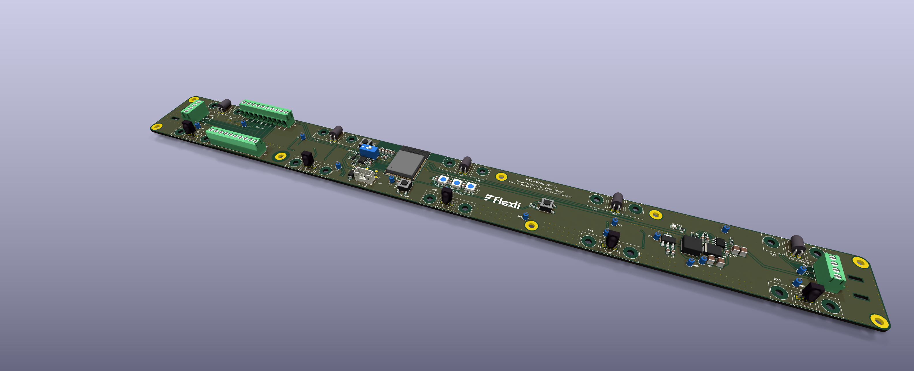
| Board | PTL-RAIL |
| Revision | rev A (v1.0) |
| Status | Released as ptl-rail-rev-a-v1.0. ERC/DRC clean; see §14 for open items |
| EDA | KiCad 10 |
| License | Private / Internal (Flexli Technologies) |
One board type, chained end to end along a rack:
TX_1…TX_5).TSOP_OUT_1…5) leave on J3 to the board below. The receivers of the board above arrive on J4 (TSOP_OUT_n_ESP) and go into the ESP32.flowchart TB
subgraph PWR["Power"]
VIN[("VIN 24 V nominal\nJ3/J4/J5/J6")] --> BUCK["TPS54360B buck\n(L1 15 uH, D1 SS36) -> +5V"]
BUCK --> LDO["TLV1117-33\nLDO -> +3V3"]
USB[("J1 USB 5V")] -->|"D3 SS14"| BUCK5(("+5V"))
end
subgraph MCU["Controller"]
ESP["ESP32-S3-WROOM-1"]
CAN["SN65HVD230 + PESD1CAN\nSW3 120R termination"]
RGB["WS2812B x3 (D4-D6)"]
ESP -->|"IO15/IO16"| CAN
ESP -->|"IO18"| RGB
end
subgraph NODES["5 nodes, 84 mm pitch"]
TX["5x IR333C + AO3400A\n(top edge)"]
RX["5x TSOP382xx\n(bottom edge)"]
end
ESP -->|"TX_1-5 (IO9-IO13)"| TX
RX -->|"TSOP_OUT_1-5 -> J3"| BELOW(["board below"])
ABOVE(["board above"]) -->|"J4 -> IO4-IO8"| ESP
CAN <-->|"CAN_H/CAN_L\nJ5/J6, J3/J4"| BUS(["CAN bus"])

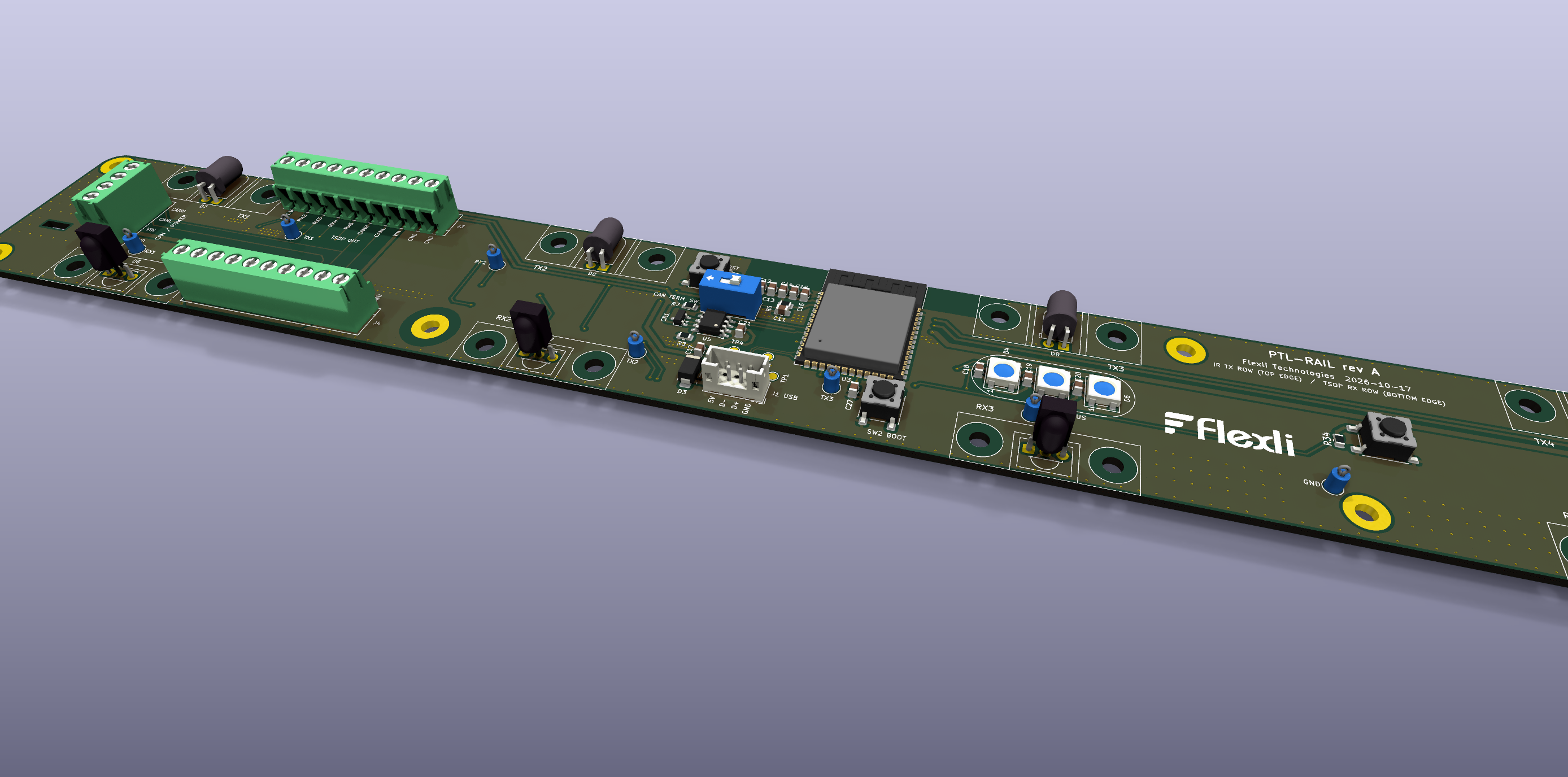
| Board | 400 × 40 mm, 2-layer FR-4, 1.6 mm. 4 mm corner radius, concentric with the corner holes |
| Nodes | 5. Centres at x = 32, 116, 200, 284, 368 mm from the left edge |
| Emitters | IR333C, 180 Ω from +5 V, AO3400A low-side switch, 100 Ω gate resistor and 100 kΩ pull-down |
| Receivers | TSOP382xx on +3V3 through 100 Ω + 4.7 µF, 100 Ω series resistor on the output |
| Controller | ESP32-S3-WROOM-1, native USB (USBLC6-2 ESD) on J1 |
| Bus | CAN, SN65HVD230, PESD1CAN, switchable 120 Ω termination (SW3 + R7) |
| User I/O | SW1 RST, SW2 BOOT, SW4 ACK_BUTTON (IO14, 10 kΩ pull-up, 100 nF), D2 power LED, D4–D6 WS2812B |
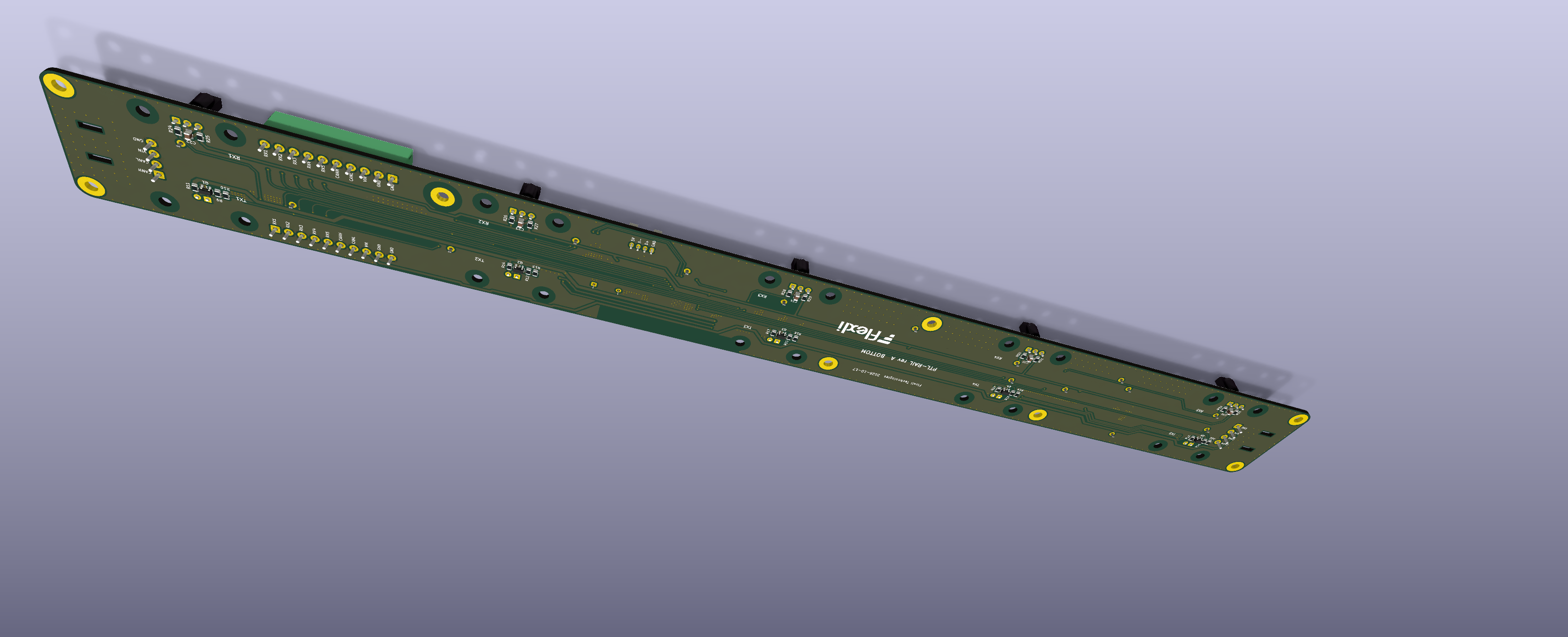
| Copper | GND pour on both layers, redundant GND vias, GND via fence along the board edge |
| Test | TP1–TP19 (loop test points on every TX/RX signal and every rail, see §10) |
Stress ratings come from the component datasheets. Rev A has no input protection (see §14), so these are the limits of the silicon itself.
| Parameter | Limiting part | Min | Max | Unit |
|---|---|---|---|---|
VIN | TPS54360B (U2) | −0.3 | 65 | V |
VIN on C1/C3 | capacitor rating, not yet specified | — | rating TBD | V |
| CAN_H / CAN_L bus pins | SN65HVD230 (U5) | −4 | 16 | V |
| +3V3 rail | ESP32-S3 / TLV1117 output | −0.3 | 3.6 | V |
| +5V rail | USBLC6-2 VBUS (U4) | −0.3 | 5.5 | V |
| Parameter | Min | Typ | Max | Unit |
|---|---|---|---|---|
VIN | 4.5 (U2) | 24 | 60 (U2), subject to C1/C3 rating | V |
| CAN data rate | — | — | 1 | Mbps |
flowchart TB
    A["Rail board N-1 (above)"] -->|"J3 -> J4\nTSOP_OUT 1-5, CAN, VIN, GND"| B["Rail board N"]
    B -->|"J3 -> J4"| C["Rail board N+1 (below)"]
    L(["neighbour on the left"]) <-->|"J5: CAN_H, CAN_L, VIN, GND"| B
    B <-->|"J6: GND, VIN, CAN_L, CAN_H"| R(["neighbour on the right"])
J3 carries this board's receiver outputs down to the next board's J4, which feeds that board's ESP32 IO4–IO8. J3/J4 also pass CAN and power. J5/J6 at the two ends of the board are mirrored 4-way CAN + power terminals for chaining along the rail. The J3 → J4 pin order is reversed (J3.1 = RX1, J4.10 = RX1), so check the harness before first power-up.
Pin labels are printed on both silkscreen sides.
| Connector | Type | Pinout (1→N) |
|---|---|---|
J3 TSOP OUT | 10-way 3.5 mm screw terminal | 1–5: RX1…RX5 (TSOP_OUT_1…5) · 6: CAN_H · 7: CAN_L · 8: VIN · 9: GND · 10: GND |
J4 TSOP IN | 10-way 3.5 mm screw terminal | 1: GND · 2: GND · 3: VIN · 4: CAN_L · 5: CAN_H · 6–10: RX5…RX1 (TSOP_OUT_5…1_ESP) |
J5 (left end) | 4-way 3.5 mm screw terminal | 1: CAN_H · 2: CAN_L · 3: VIN · 4: GND |
J6 (right end) | 4-way 3.5 mm screw terminal | 1: GND · 2: VIN · 3: CAN_L · 4: CAN_H |
J1 USB | JST-PH 4-way | 1: GND · 2: D+ · 3: D− · 4: 5V (VBUS, via D3) |
SW3 | slide DIP | ON = 120 Ω (R7) across CAN_H/CAN_L |
| Pin # | Pin name | Net / function |
|---|---|---|
| 1 | GND | Ground |
| 2 | 3V3 | 3.3 V supply |
| 3 | EN | ESP_EN, reset (SW1) |
| 4 | IO4 | TSOP_OUT_1_ESP (J4.10) |
| 5 | IO5 | TSOP_OUT_2_ESP (J4.9) |
| 6 | IO6 | TSOP_OUT_3_ESP (J4.8) |
| 7 | IO7 | TSOP_OUT_4_ESP (J4.7) |
| 8 | IO15 | CAN_TX |
| 9 | IO16 | CAN_RX |
| 10 | IO17 | unused |
| 11 | IO18 | STATUS_LED (WS2812B DIN, D4→D5→D6) |
| 12 | IO8 | TSOP_OUT_5_ESP (J4.6) |
| 13 | IO19 | USB_D- |
| 14 | IO20 | USB_D+ |
| 15 | IO3 | unused (strap pin) |
| 16 | IO46 | unused (strap pin) |
| 17 | IO9 | TX_1 (emitter node 1) |
| 18 | IO10 | TX_2 |
| 19 | IO11 | TX_3 |
| 20 | IO12 | TX_4 |
| 21 | IO13 | TX_5 |
| 22 | IO14 | ACK_BUTTON (SW4) |
| 23–25 | IO21, IO47, IO48 | unused |
| 26 | IO45 | unused, no-connect (VDD_SPI strap; keep low at boot) |
| 27 | IO0 | GPIO0, BOOT (SW2) |
| 28–35 | IO35–IO42 | unused |
| 36, 37 | RXD0, TXD0 | unused (UART0 debug) |
| 38, 39 | IO2, IO1 | unused (ADC-capable) |
| 40, 41 | GND | Ground / thermal pad |
| TP | Net | Footprint |
|---|---|---|
| TP1 / TP2 | USBC_D+ / USBC_D− (connector side) | SMD pad Ø1.5 mm |
| TP3 / TP4 | USB_D+ / USB_D− (ESP32 side) | SMD pad Ø1.5 mm |
| TP5 … TP9 | TX_1 … TX_5 | Loop Ø1.8 mm, drill 1.0 mm |
| TP10 … TP14 | TSOP_OUT_1 … TSOP_OUT_5 | Loop Ø1.8 mm, drill 1.0 mm |
| TP15 / TP16 / TP17 | VIN / +5V / +3V3 | Loop Ø1.8 mm, drill 1.0 mm |
| TP18 / TP19 | GND | Loop Ø1.8 mm, drill 1.0 mm |
Fabrication
Assembly
The production files are attached to each GitHub release. The current release is ptl-rail-rev-a-v1.0:
| Asset | File |
|---|---|
| Bill of Materials | PTL-RAIL_revA_BOM.csv (grouped by Value + Footprint; test points and holes excluded) |
| Gerbers + drill files (fabrication, 2-board panel) | PTL-RAIL_revA_gerbers_drill_panel-2up.zip (with panel pick-and-place in assembly/) |
| Interactive BOM | PTL-RAIL_revA_ibom.html |
| IPC netlist | PTL-RAIL_revA_netlist.ipc (IPC-D-356) |
| Pick-and-place position file | PTL-RAIL_revA_pick-and-place.csv (single board, both sides, mm) |
| Reference designator list | PTL-RAIL_revA_refdes.csv |
| Schematic (PDF plot) | PTL-RAIL_revA_schematic.pdf |
| Schematic (KiCad source) | PTL-RAIL_revA_kicad-source.zip (project, sheets, PCB, libraries, 3D models, panel PCB) |
| 3D model (STEP) | PTL-RAIL_revA_step.zip → PTL-RAIL_revA.step (board, components, copper, silkscreen; ~40 MB unzipped) |
.
├── README.md                      This file
└── PTL-RAIL/
    ├── PTL-RAIL.kicad_pro         KiCad project
    ├── PTL-RAIL.kicad_sch         Root sheet
    ├── PTL-RAIL.kicad_pcb         Board layout
    ├── esp32.kicad_sch            ESP32-S3, USB, buttons, status LEDs, test points
    ├── power.kicad_sch            TPS54360B buck, TLV1117 LDO
    ├── can.kicad_sch              SN65HVD230 CAN interface
    ├── connectors.kicad_sch       J3/J4/J5/J6
    ├── tx_nodes.kicad_sch         5x IR emitter + MOSFET
    ├── rx_nodes.kicad_sch         5x TSOP receiver
    ├── lib/                       Project symbols, footprints (0_IC) and 3D models
    └── Docs/
        ├── datasheets/            Component datasheets
└── renders/ Board renders used in this README| Revision | Date | Notes |
|---|---|---|
| rev A scaffold | 2026-10-17 | KiCad project skeleton: outline, holes, node markers, sheets. |
| rev A placement | 2026-10-17 | LED row on the top edge, TSOP row on the bottom edge, node parts at 84 mm pitch, J3/J4 10-way and J5/J6 4-way terminals, CAN block, buttons, status LEDs, mounting holes. |
| rev A layout | 2026-10-18 | IR shroud outlines and holes, node parts moved to the bottom side, routing with filleted bus, GND vias and edge via fence, silkscreen cleanup, mid-board holes, rounded corners, test points TP5–TP19, SW4 ACK button on IO14. |
| rev A v1.0 | 2026-10-18 | Values normalised, ERC/DRC clean, 3D models, production files and release ptl-rail-rev-a-v1.0. |
© Flexli Technologies. Private / internal.
| Qty | Value | Footprint | References |
|---|---|---|---|
| 20 | MountingHole_3.2mm_M3 | MountingHole:MountingHole_3.2mm_M3 | H5, H10, H11, H12, H13, H14, H15, H16, H17, H18, H19, H20, H21, H22, H23, H24 +4 |
| 15 | 100R | Resistor_SMD:R_0805_2012Metric | R9, R12, R15, R18, R21, R24, R25, R26, R27, R28, R29, R30, R31, R32, R33 |
| 9 | 100nF | Capacitor_SMD:C_0805_2012Metric | C5, C10, C16, C17, C18, C19, C20, C21, C27 |
| 8 | MountingHole_M3 | MountingHole:MountingHole_3.2mm_M3_Pad | H1, H2, H3, H4, H25, H26, H27, H28 |
| 5 | 100k | Resistor_SMD:R_0805_2012Metric | R10, R13, R16, R19, R22 |
| 5 | 180R | Resistor_SMD:R_0805_2012Metric | R11, R14, R17, R20, R23 |
| 5 | 4.7uF | Capacitor_SMD:C_0805_2012Metric | C22, C23, C24, C25, C26 |
| 5 | AO3400A | Package_TO_SOT_SMD:SOT-23 | Q1, Q2, Q3, Q4, Q5 |
| 5 | IR333C | LED_THT:LED_D5.0mm_Horizontal_O1.27mm_Z3.0mm_IRGrey | D7, D8, D9, D10, D11 |
| 5 | TSOP382xx | OptoDevice:Vishay_MINICAST-3Pin | U6, U7, U8, U9, U10 |
| 4 | 10uF | Capacitor_SMD:C_0805_2012Metric | C2, C4, C12, C13 |
| 3 | 10k | Resistor_SMD:R_0805_2012Metric | R6, R8, R34 |
| 3 | SW_SPST | Button_Switch_SMD:SW_SPST_PTS645Sx43SMTR92 | SW1, SW2, SW4 |
| 3 | WS2812B | LED_SMD:LED_WS2812B_PLCC4_5.0x5.0mm_P3.2mm | D4, D5, D6 |
| 2 | 1uF | Capacitor_SMD:C_0805_2012Metric | C11, C15 |
| 2 | 2.2uF | Capacitor_SMD:C_1210_3225Metric | C1, C3 |
| 2 | 22uF | Capacitor_SMD:C_1210_3225Metric | C8, C9 |
| 2 | GND | TestPoint:TestPoint_Loop_D1.80mm_Drill1.0mm_Beaded | TP18, TP19 |
| 2 | LOGO | LOGO | G***, G*** |
| 2 | Screw_Terminal_01x04 | TerminalBlock_4Ucon:TerminalBlock_4Ucon_1x04_P3.50mm_Horizontal | J5, J6 |
| 2 | Screw_Terminal_01x10 | TerminalBlock_4Ucon:TerminalBlock_4Ucon_1x10_P3.50mm_Horizontal | J3, J4 |
| 1 | +3V3 | TestPoint:TestPoint_Loop_D1.80mm_Drill1.0mm_Beaded | TP17 |
| 1 | +5V | TestPoint:TestPoint_Loop_D1.80mm_Drill1.0mm_Beaded | TP16 |
| 1 | 100pF | Capacitor_SMD:C_0805_2012Metric | C7 |
| 1 | 11.5k | Resistor_SMD:R_0805_2012Metric | R4 |
| 1 | 120R | Resistor_SMD:R_0805_2012Metric | R7 |
| 1 | 15uH | Inductor_SMD:L_APV_ANR8040 | L1 |
| 1 | 1k | Resistor_SMD:R_0805_2012Metric | R5 |
| 1 | 22nF | Capacitor_SMD:C_0805_2012Metric | C6 |
| 1 | 22uF | Capacitor_SMD:C_0805_2012Metric | C14 |
| 1 | 274k | Resistor_SMD:R_0805_2012Metric | R1 |
| 1 | 60.4k | Resistor_SMD:R_0805_2012Metric | R3 |
| 1 | 8.45k | Resistor_SMD:R_0805_2012Metric | R2 |
| 1 | ESP32-S3-WROOM-1 | RF_Module:ESP32-S3-WROOM-1 | U3 |
| 1 | JST_PH_4P | Connector_JST:JST_PH_B4B-PH-K_1x04_P2.00mm_Vertical | J1 |
| 1 | LED | LED_SMD:LED_0805_2012Metric | D2 |
| 1 | PESD1CAN_215 | Package_TO_SOT_SMD:SOT-23 | CR1 |
| 1 | SN65HVD230DR | Package_SO:SOIC-8_3.9x4.9mm_P1.27mm | U5 |
| 1 | SS14 | Diode_SMD:D_SMA | D3 |
| 1 | SS36 | Diode_SMD:D_SMC | D1 |
| 1 | SW_DIP_x01 | Button_Switch_THT:SW_DIP_SPSTx01_Slide_9.78x4.72mm_W7.62mm_P2.54mm | SW3 |
| 1 | TLV1117-33 | Package_TO_SOT_SMD:SOT-223-3_TabPin2 | U1 |
| 1 | TPS54360BQDDARQ1 | 0_IC:TPS54360BQDDARQ1 | U2 |
| 1 | TSOP_OUT_1 | TestPoint:TestPoint_Loop_D1.80mm_Drill1.0mm_Beaded | TP10 |
| 1 | TSOP_OUT_2 | TestPoint:TestPoint_Loop_D1.80mm_Drill1.0mm_Beaded | TP11 |
| 1 | TSOP_OUT_3 | TestPoint:TestPoint_Loop_D1.80mm_Drill1.0mm_Beaded | TP12 |
| 1 | TSOP_OUT_4 | TestPoint:TestPoint_Loop_D1.80mm_Drill1.0mm_Beaded | TP13 |
| 1 | TSOP_OUT_5 | TestPoint:TestPoint_Loop_D1.80mm_Drill1.0mm_Beaded | TP14 |
| 1 | TX_1 | TestPoint:TestPoint_Loop_D1.80mm_Drill1.0mm_Beaded | TP5 |
| 1 | TX_2 | TestPoint:TestPoint_Loop_D1.80mm_Drill1.0mm_Beaded | TP6 |
| 1 | TX_3 | TestPoint:TestPoint_Loop_D1.80mm_Drill1.0mm_Beaded | TP7 |
| 1 | TX_4 | TestPoint:TestPoint_Loop_D1.80mm_Drill1.0mm_Beaded | TP8 |
| 1 | TX_5 | TestPoint:TestPoint_Loop_D1.80mm_Drill1.0mm_Beaded | TP9 |
| 1 | USBC_D+ | TestPoint:TestPoint_Pad_D1.5mm | TP1 |
| 1 | USBC_D- | TestPoint:TestPoint_Pad_D1.5mm | TP2 |
| 1 | USBLC6-2SC6 | Package_TO_SOT_SMD:SOT-23-6 | U4 |
| 1 | USB_D+ | TestPoint:TestPoint_Pad_D1.5mm | TP3 |
| 1 | USB_D- | TestPoint:TestPoint_Pad_D1.5mm | TP4 |
| 1 | VIN | TestPoint:TestPoint_Loop_D1.80mm_Drill1.0mm_Beaded | TP15 |
Fayeinstainy/BIR25_TEAM_E
Biorobitics for team E: smart ant swarm robots inspired from Formica


electromotif208/pcb-portfolio
👨💻 Electronics Engineer 📺 YouTube: ELECTROMOTIF 🔧 Tools: KiCad, EasyEDA 📡 Domains: Power Supply, ESP32, IoT, Embedded Hardware


WestianPKl/pcb-docs
A collection of custom PCB designs created in KiCAD, centered around the Raspberry Pi Pico (RP2040) platform. Each board is a standalone module that connects to the Main Board and extends its functionality via I2C, SPI…

jliusgustalvoo/making-pcb-with-esp32-s3-with-sensor-actuator-i2c-pin
making pcb with esp32-s3 with sensor,actuator,i2c pin for college task

enkhbold470/iron-node
ESP32-S3 industrial gateway: W5500 Ethernet, isolated RS-485 (ADM2587E), CAN, 9-36 V input. 4-layer KiCad 10 board.
It measures 400 × 40 mm and has 2 copper layers, 1.6 mm thick.
147 parts, built around the ESP32-S3-WROOM-1-N8, SN65HVD230DR, TPS54360BQDDARQ1 and TLV1117-33DCY. The full list of its parts is on this page, with links to each part's symbol and footprint where PCBKit's library has them.
From the mayoogh-flexli/Meesho-Put-To-Light repository on GitHub, at the commit this page was made from: the board is PTL-RAIL/PTL-RAIL.kicad_pcb and its schematic PTL-RAIL/PTL-RAIL.kicad_sch. PCBKit opens the board in the browser, with nothing to install.
Its repository states no licence, so its author keeps all rights: ask mayoogh-flexli before reusing the design.