2 layers34 × 96 mm
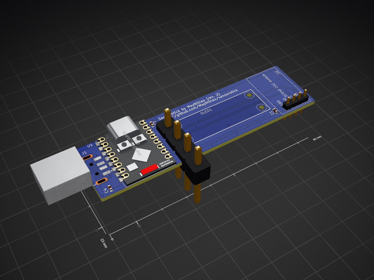
 MayNiklas/sensorstick2
a compact PCB designed to integrate a CO2 sensor into a USB stick form factor
Sensorstick is an open-source printed circuit board by MayNiklas, from the MayNiklas/sensorstick repository on GitHub. It is a 2-layer board of 85 × 23 mm with 8 parts on 19 nets, routed with 55 tracks and 45 vias.
It is built around the HS91L02W2C01. Its parts include 4 capacitors, 2 ICs and 1 connector. It belongs with the sensors and measurement boards and the ESP32 and RISC-V boards of this library.
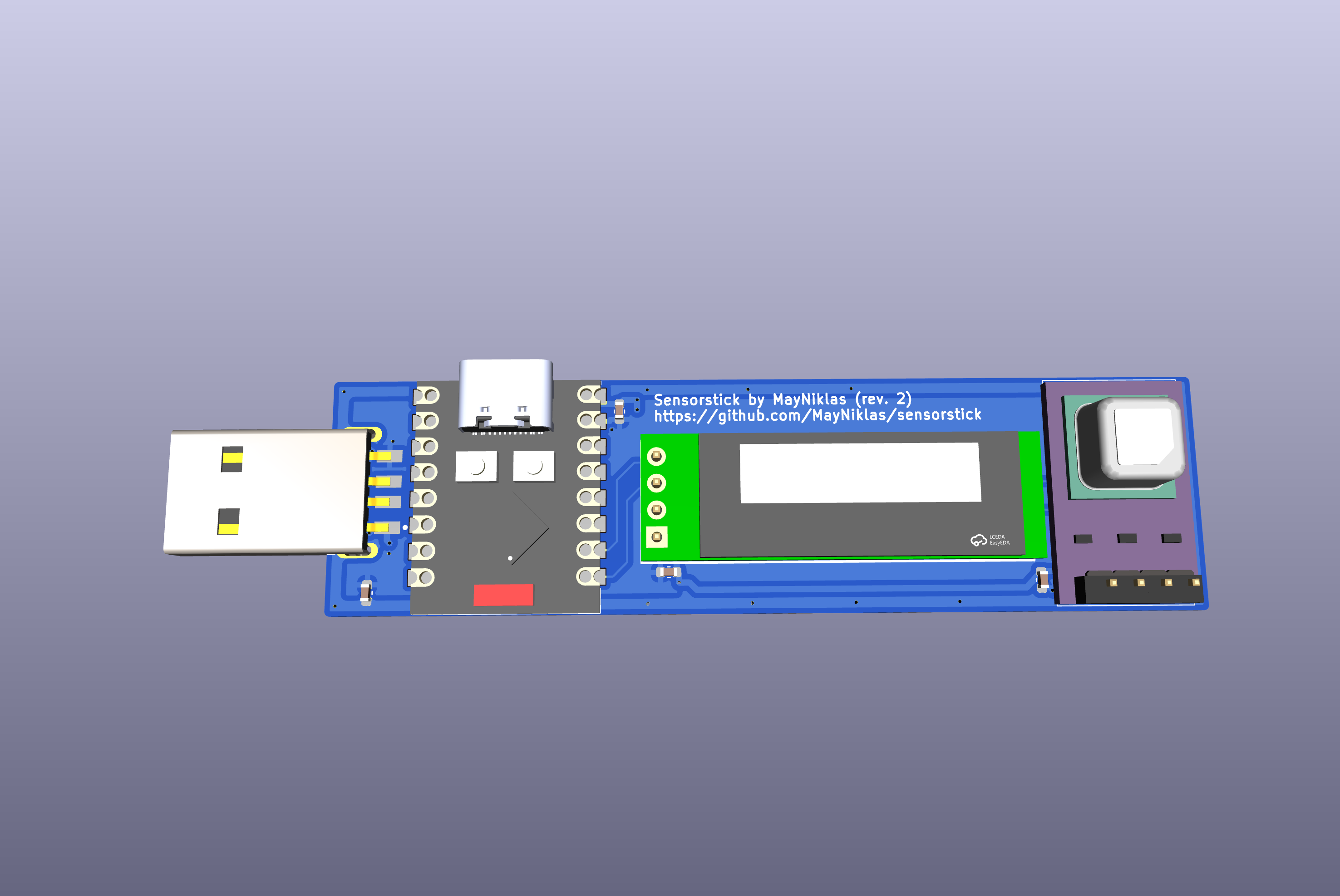
Interactive BOM: https://mayniklas.github.io/sensorstick/
| Qty | Value | Footprint | References |
|---|---|---|---|
| 4 | 100nF | Capacitor_SMD:C_0603_1608Metric | C1, C2, C3, C4 |
| 1 | ESP32-C3_SUPERMINI | CustomLibrary:ESP32-C3_SUPERMINI_SMD | U1 |
| 1 | HS91L02W2C01 | CustomLibrary:OLED-TH_L38.0-W12.0_HS91L02W2C01 | OLED1 |
| 1 | SCD40 CO2 module | CustomLibrary:SCD40_CO2_module | U2 |
| 1 | U217-04XN-XXR84 | CustomLibrary:USB-A-SMD_U217-041N-4BV81 | J1 |
It measures 85 × 23 mm and has 2 copper layers, 1.6 mm thick.
8 parts, built around the HS91L02W2C01. The full list of its parts is on this page, with links to each part's symbol and footprint where PCBKit's library has them.
From the MayNiklas/sensorstick repository on GitHub, at the commit this page was made from: the board is sensorstick/sensorstick.kicad_pcb and its schematic sensorstick/sensorstick.kicad_sch. PCBKit opens the board in the browser, with nothing to install.
Its repository states no licence, so its author keeps all rights: ask MayNiklas before reusing the design.


pranay-k4/BuildPad
A customizable open-source macropad for makers, coders, designers, and electronics builders.

EDA-bench/eda-bench
Execution-based benchmark for open-book KiCad PCB reconstruction agents

laforestlabs/KiCraft
KiCad PCB automation toolkit — placement, routing, scoring, and experiment management
