2 layers18.5 × 11.1 mm
Switch
byrantech/laptop
anyon_e, a highly integrated, high end, open source laptop. Attempt the impossible.
6 parts4.3kMIT

 matthias-bs/peripheral-load-switch1
MCU Peripheral Load Switch
Load switch is an open-source printed circuit board by matthias-bs, from the matthias-bs/peripheral-load-switch repository on GitHub. It is a 2-layer board of 25.4 × 14 mm with 6 parts on 5 nets, routed with 37 tracks and 5 vias.
Its parts include 2 connectors, 1 resistor and 1 IC.

Compact SMD peripheral load switch based on the Vishay SiP32431, designed for enabling/disabling power to microcontroller peripherals.
A minimal, all-SMD load switch board for switching a peripheral's supply voltage under microcontroller control. The design uses the Vishay SiP32431DR3 high-side switch in a SC-70-6 (SOT-363) package. Board-edge castellated contacts (J2, half-hole, DNP) allow direct PCB-to-PCB soldering or surface mounting. An optional 5-pin 2.54 mm pitch pin header (J1) provides access for prototyping with breadboards or Dupont wires.
Datasheet: SiP32431 (Vishay, PDF)
| Parameter | Value |
|---|---|
| Operating voltage | 1.5 V – 5.5 V |
| Max continuous current | 1.2 A |
| RDS(on) | 147 mΩ |
| Package | SC-70-6 (JEITA) / SOT-363 (JEDEC) |
| Enable logic | Active-high |
| Switch type | High-side |
| Leakage current | 10 pA (ultra-low) |
| Special features | Reverse current blocking, soft-start, ultra-low quiescent current |
Edge_HalfHole_5Pin_2.54mm footprint included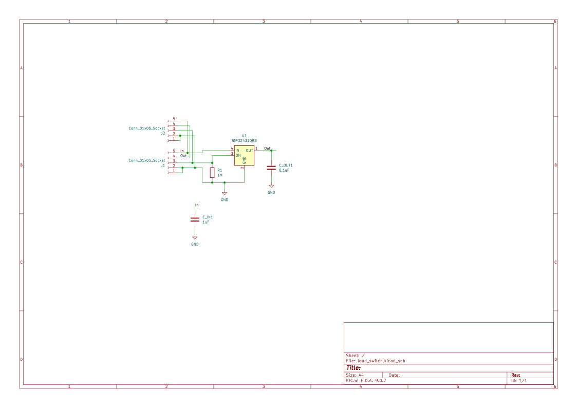
Click image to open interactive schematic viewer (KiCanvas)
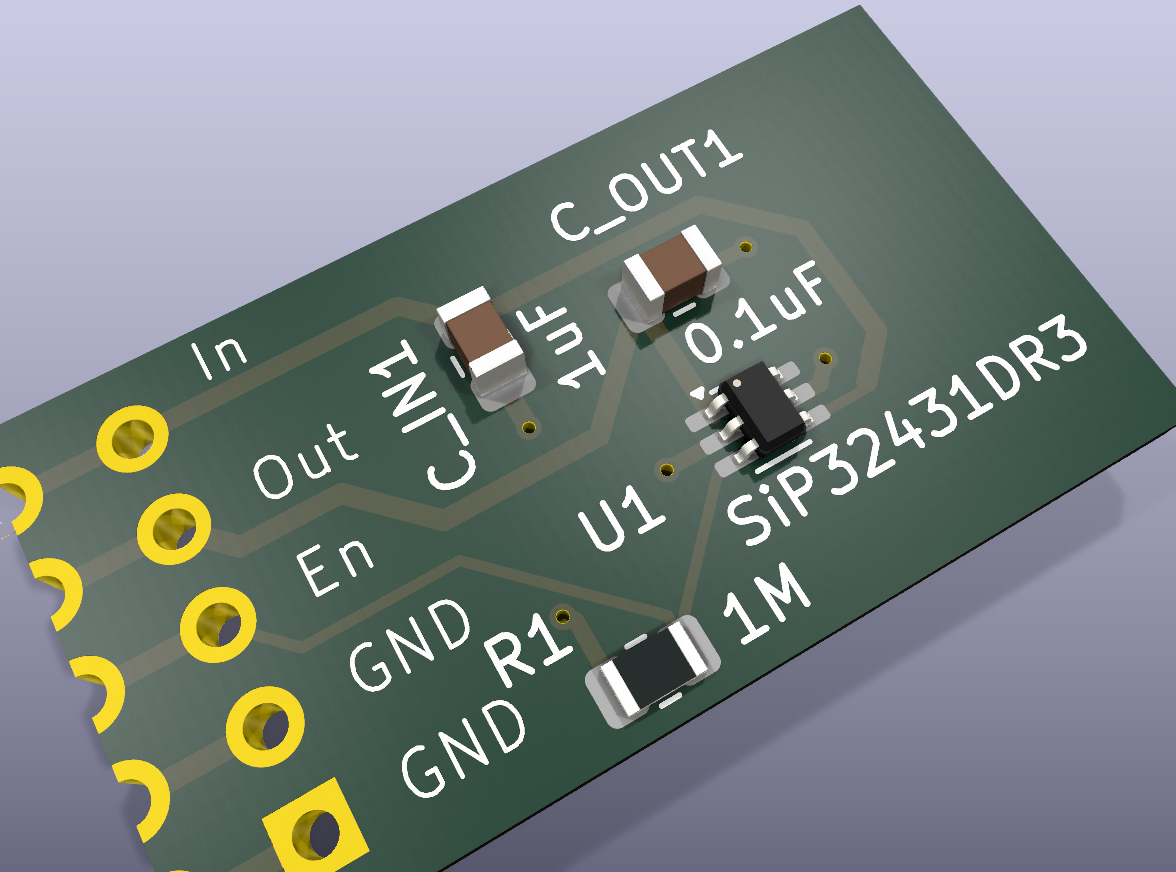
Click image to open the interactive 3D model viewer (rotate/zoom/pan) — or use KiCanvas for a full PCB layer inspector
How it was generated: The 3D model (
docs/load_switch.glb) was exported from KiCad 9 usingkicad-cli pcb export glbwith tracks, pads, zones, silkscreen and soldermask included. The viewer (docs/index.html) is a custom Three.js page served via GitHub Pages.
| Ref | Value | Footprint | Description | LCSC Part # |
|---|---|---|---|---|
| U1 | SiP32431DR3 | SC-70-6 (SOT-363) | High-side load switch | C141606 |
| R1 | 1 MΩ | 0805 | Pull-down on EN pin | C17514 |
| C_IN1 | 1 µF | 0805 | Input decoupling capacitor | C1712 |
| C_OUT1 | 100 nF | 0805 | Output decoupling capacitor | C126469 |
| J1 | — | PinSocket 1×5 2.54 mm | Optional pin header | — |
| J2 | — | Half-hole 5-pin 2.54 mm (DNP¹) | Edge connector | — |
¹ DNP = Do Not Populate — the half-hole edge connector (J2) is a PCB manufacturing feature: the through-holes are routed in half at the board edge to form castellated contacts. No separate component is soldered.
LCSC Part # are ordering references for lcsc.com.
| Pin | Signal | Description |
|---|---|---|
| 1 | GND | Ground |
| 2 | GND | Ground |
| 3 | EN | Enable (active-high) |
| 4 | OUT | Switched output |
| 5 | IN | Supply voltage input |
Ready-to-order Gerber files (standard RS-274X, compatible with any PCB fab) are in the production/ folder.
Copyright 2026 Matthias Prinke
SPDX-License-Identifier: Apache-2.0 WITH SHL-2.1
Licensed under the Solderpad Hardware License v2.1. See LICENSE for the full text.
| Qty | Value | Footprint | References |
|---|---|---|---|
| 1 | 0.1uF | Capacitor_SMD:C_0805_2012Metric | C_OUT1 |
| 1 | 1M | Resistor_SMD:R_0805_2012Metric | R1 |
| 1 | 1uF | Capacitor_SMD:C_0805_2012Metric | C_IN1 |
| 1 | Conn_01x05_Socket | Connector_PinSocket_2.54mm:PinSocket_1x05_P2.54mm_Vertical | J1 |
| 1 | Conn_01x05_Socket | MyCustom:Edge_HalfHole_5Pin_2.54mm | J2 |
| 1 | SiP32431DR3 | Package_TO_SOT_SMD:SOT-363_SC-70-6 | U1 |
byrantech/laptop
anyon_e, a highly integrated, high end, open source laptop. Attempt the impossible.


Jcparkyn/dpoint
Open-source digital stylus using camera tracking and inertial measurements

VoronDesign/Voron-Hardware
Cool Hardware designed by the Voron Design group

hoglet67/RGBtoHDMI
Bare-metal Raspberry Pi project that provides pixel-perfect sampling of Retro Computer RGB/YUV video and conversion to HDMI

hackclub/OnBoard
💡 Join 1,000 teenagers and make your first PCB with a $100 grant!

Luos-io/luos_engine
Open-source and real-time orchestrator for cyber-physical-systems, to easily design, test and deploy embedded applications and digital twins.

It measures 25.4 × 14 mm and has 2 copper layers, 1.6 mm thick.
6 parts. The full list of its parts is on this page, with links to each part's symbol and footprint where PCBKit's library has them.
From the matthias-bs/peripheral-load-switch repository on GitHub, at the commit this page was made from: the board is load_switch.kicad_pcb and its schematic load_switch.kicad_sch. PCBKit opens the board in the browser, with nothing to install.
Its repository states no licence, so its author keeps all rights: ask matthias-bs before reusing the design.