4 layers100 × 120 mm
 math-milan/PowerbankTestCode2
This is a firmware for a Powerbank testboard where i want to evealuate multiple ti chips like the tps25751
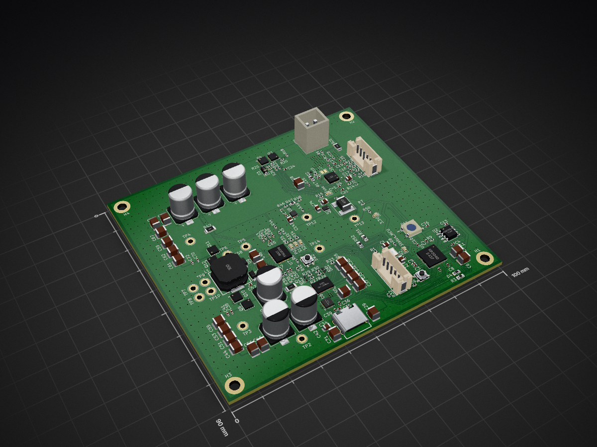
Powerbank devboard is an open-source printed circuit board by math-milan, from the math-milan/PowerbankTestCode repository on GitHub, published under the MIT licence. It is a 2-layer board of 100 × 90 mm with 185 parts on 155 nets, routed with 1,350 tracks and 638 vias.
It is built around the RP2040, W25Q128JVSIQ and BQ40Z80RSMR, with the TPD6S300ARUK, CSD15380F3 and CSD25480F3 among its other parts. Its parts include 76 capacitors, 52 resistors, 11 diodes, 11 transistors and 8 ICs. It belongs with the power and microcontroller boards boards and the RP2040 boards of this library.


In order to build the *.uf2 file, which then can be transferred to the RP2040 by copying it to the virtual disk:
mkdir build
cd build
cmake ..
The file will be called main.uf2.
sudo src/openocd -s tcl -f interface/cmsis-dap.cfg -f target/rp2040.cfg -c "adapter speed 5000"
| Qty | Value | Footprint | References |
|---|---|---|---|
| 28 | 100nF | SMD_Capacitors:C_0402 | C3, C4, C10, C11, C12, C13, C16, C17, C18, C19, C20, C22, C25, C39, C41, C45 +12 |
| 10 | 10k | SMD_Resistors:R_0402_1005Metric | R6, R16, R20, R24, R31, R32, R33, R34, R35, R39 |
| 10 | 10uF | SMD_Capacitors:C_1210_3225Metric | C30, C32, C33, C37, C53, C55, C56, C59, C61, C62 |
| 7 | 100 | SMD_Resistors:R_0402_1005Metric | R10, R11, R12, R13, R14, R19, R22 |
| 7 | 100pF | SMD_Capacitors:C_0402 | C15, C21, C23, C24, C26, C38, C72 |
| 7 | 4.7uF | SMD_Capacitors:C_1210_3225Metric | C29, C46, C48, C51, C52, C64, C67 |
| 6 | 1k | SMD_Resistors:R_0402_1005Metric | R1, R2, R8, R9, R26, R50 |
| 6 | 1uF | SMD_Capacitors:C_1210_3225Metric | C5, C6, C28, C43, C44, C68 |
| 6 | 56uF | CAP_SMD_POLARIZED:CP_Elec_8x10.5 | C40, C42, C54, C60, C69, C71 |
| 6 | AOS AON7318 | easyeda2kicad:DFN-8_L3.3-W3.3-P0.65-BL-3 | Q3, Q4, Q9, Q10, Q11, Q12 |
| 4 | 10 | SMD_Resistors:R_0402_1005Metric | R36, R38, R41, R43 |
| 4 | 100k | SMD_Resistors:R_0402_1005Metric | R15, R27, R29, R49 |
| 4 | 1M | SMD_Resistors:R_0402_1005Metric | R18, R25, R28, R30 |
| 4 | MountingHole_Pad | MountingHole:MountingHole_3.2mm_M3_ISO7380_Pad_TopBottom | H1, H2, H3, H4 |
| 3 | 5k | SMD_Resistors:RC_0805 | R17, R51, R52 |
| 3 | CSD15380F3 | powerbank_footprints:PICOSTAR-3_L0.7-W0.6-P0.35-TL | Q1, Q2, Q5 |
| 2 | 0R | SMD_Resistors:R_0402_1005Metric | R5, R7 |
| 2 | 220pF | SMD_Capacitors:C_0402 | C35, C36 |
| 2 | 22pF | SMD_Capacitors:C_0805 | C1, C2 |
| 2 | 22uF | SMD_Capacitors:C_0805 | C74, C75 |
| 2 | 27 | SMD_Resistors:RC_0805 | R3, R4 |
| 2 | 470nF | SMD_Capacitors:C_0402 | C47, C65 |
| 2 | 5m | SMD_Resistors:RC_1206 | R37, R42 |
| 2 | CSD25480F3 | powerbank_footprints:PICOSTAR-3_L0.7-W0.6-P0.40-TL | Q6, Q13 |
| 2 | V1FM10-M3/H | powerbank_footprints:SOD-123_L2.8-W1.8-LS3.7-RD | D8, D9 |
| 1 | 0 | SMD_Resistors:R_0402_1005Metric | R40 |
| 1 | 10nF | SMD_Capacitors:C_0805 | C34 |
| 1 | 10nF | SMD_Capacitors:C_1210_3225Metric | C31 |
| 1 | 10uH | powerbank_footprints:IND-SMD_L10.0-W10.0-1 | L1 |
| 1 | 12MHz | Crystals_and_Oscillators:C9002 | Y1 |
| 1 | 17.5k | SMD_Resistors:RC_0603 | R47 |
| 1 | 1m | SMD_Resistors:RC_1206 | R21 |
| 1 | 1uF | SMD_Capacitors:C_0805 | C14 |
| 1 | 2.2uF | SMD_Capacitors:C_0805 | C27 |
| 1 | 22k | SMD_Resistors:R_0402_1005Metric | R46 |
| 1 | 249k | SMD_Resistors:R_0402_1005Metric | R44 |
| 1 | 280k | SMD_Resistors:R_0402_1005Metric | R48 |
| 1 | 3.3V | TestPoint:TestPoint_Loop_D2.60mm_Drill1.6mm_Beaded | TP13 |
| 1 | 3.3V | Leds:LED_0603 | D10 |
| 1 | 4.7uH | powerbank_footprints:IND-SMD_L6.0-W6.0_CR6045 | L2 |
| 1 | 510 | SMD_Resistors:R_0402_1005Metric | R23 |
| 1 | 5V | TestPoint:TestPoint_Loop_D2.60mm_Drill1.6mm_Beaded | TP14 |
| 1 | 9.42k | SMD_Resistors:R_0402_1005Metric | R45 |
| 1 | BQ25756 | Package_DFN_QFN:RRV0036A | U7 |
| 1 | BQ40Z80RSMR | Package_DFN_QFN:RSM0032A-IPC_A | U4 |
| 1 | Ballance Conn | Connector_JST:CONN-SMD_5P-P2.00_B6B-PH-SM4-TB-LF-SN | J2 |
| 1 | Conn_01x02_Pin | Connector_Wago:Wago_734-132_1x02_P3.50mm_Vertical | J4 |
| 1 | Conn_01x02_Pin | Jumper:SolderJumper-2_P1.3mm_Open_Pad1.0x1.5mm | J3 |
| 1 | Conn_01x05_Pin | Connector_JST:CONN-SMD_5P-P2.00_B6B-PH-SM4-TB-LF-SN | J1 |
| 1 | Fuse | Leds:LED_0603 | D2 |
| 1 | I-HI | TestPoint:TestPoint_Loop_D2.60mm_Drill1.6mm_Beaded | TP8 |
| 1 | I-L | TestPoint:TestPoint_Loop_D2.60mm_Drill1.6mm_Beaded | TP10 |
| 1 | I-LO | TestPoint:TestPoint_Loop_D2.60mm_Drill1.6mm_Beaded | TP7 |
| 1 | IN | TestPoint:TestPoint_Loop_D2.60mm_Drill1.6mm_Beaded | TP3 |
| 1 | MMSZ5246B | Diode_SMD:D_SOD-123 | D3 |
| 1 | O-HI | TestPoint:TestPoint_Loop_D2.60mm_Drill1.6mm_Beaded | TP5 |
| 1 | O-L | TestPoint:TestPoint_Loop_D2.60mm_Drill1.6mm_Beaded | TP9 |
| 1 | O-LO | TestPoint:TestPoint_Loop_D2.60mm_Drill1.6mm_Beaded | TP6 |
| 1 | OUT | TestPoint:TestPoint_Loop_D2.60mm_Drill1.6mm_Beaded | TP4 |
| 1 | PD-GPIO | Leds:LED_0603 | D5 |
| 1 | PG | Leds:LED_0603 | D4 |
| 1 | PPHV | TestPoint:TestPoint_Loop_D2.60mm_Drill1.6mm_Beaded | TP2 |
| 1 | RESET | Tactile_Switches:C2888419 | SW1 |
| 1 | RP2040 | Package_DFN_QFN:QFN-56-1EP_7x7mm_P0.4mm_EP3.2x3.2mm_ThermalVias | U1 |
| 1 | S1 | Leds:LED_0603 | D7 |
| 1 | S2 | Leds:LED_0603 | D6 |
| 1 | SGM6036-3.3 | Package_DFN_QFN:UTDFN-6_L2.0-W1.5-P0.50-BL-EP | U9 |
| 1 | Status_MCU | Leds:LED_0603 | D1 |
| 1 | TPD6S300A | Package_DFN_QFN:WQFN-20-1EP_3x3mm_P0.4mm_EP1.7x1.7mm | U6 |
| 1 | TPS25751D | Package_DFN_QFN:Texas_REF0038A_WQFN-38-2EP_6x4mm_P0.4 | U5 |
| 1 | TPS25961DRVR | Package_DFN_QFN:DRV0006A-IPC_A | U8 |
| 1 | TYPE-C-31-M-12 | Connector_USB:USB-C_SMD-TYPE-C-31-M-12 | USBC1 |
| 1 | VIN | TestPoint:TestPoint_Loop_D2.60mm_Drill1.6mm_Beaded | TP12 |
| 1 | VREG | TestPoint:TestPoint_Pad_1.5x1.5mm | TP1 |
| 1 | W25Q128JVS | Package_SO:SOIC-8_3.9x4.9mm_P1.27mm | U2 |
| 1 | WS2812E | Leds:C2843785 | D11 |
| 1 | {Funktion} | Tactile_Switches:C2888419 | SW2 |
It measures 100 × 90 mm and has 2 copper layers, 1.6 mm thick.
185 parts, built around the RP2040, W25Q128JVSIQ, BQ40Z80RSMR and TPD6S300ARUK. The full list of its parts is on this page, with links to each part's symbol and footprint where PCBKit's library has them.
From the math-milan/PowerbankTestCode repository on GitHub, at the commit this page was made from: the board is pcb/Rev0.1/powerbank_devboard.kicad_pcb and its schematic pcb/Rev0.1/bms.kicad_sch. PCBKit opens the board in the browser, with nothing to install.
Its repository publishes it under the MIT licence: you may reuse it on that licence's terms (keep the author's notice, and for a copyleft licence share your changes alike).


Vedatori/Time-O-Mat
Addressable LED clock kit aimed for usage in STEM education. The ultimate solution to time telling...

LimesKey/parsnip-node
A portable LoRa communicator. Custom 4-layer PCB (ESP32-S3 + E22P-915M30S LoRa + NEO-M9N GNSS), designed in KiCad for 915 MHz.


pauliano22/haven-dev-board-kicad
Haven — KiCad port of the dev board (nRF5340 + ADAU1860 DSP), based on the stock OpenEarable 2.0 design
