2 layers370.8 × 298.5 mm
8 Bit Computer
The-Invent0r/8-bit-Computer-PCB
These are the KiCAD files for my 8-Bit Computer.
323 parts142
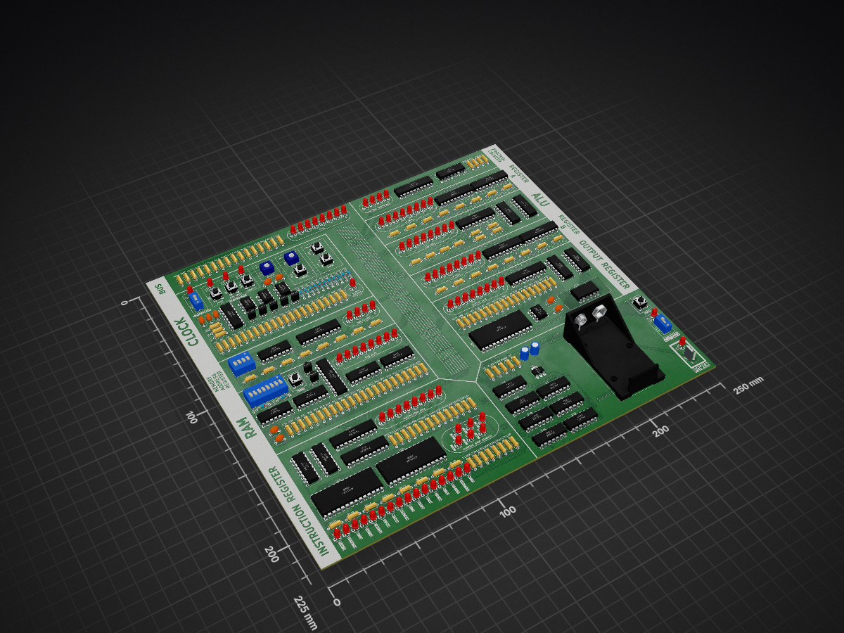
 MatanBright/8BitComputer2
This is a simple programmable 8-bit computer that is built from scratch.
8BitComputer is an open-source printed circuit board by MatanBright, from the MatanBright/8BitComputer repository on GitHub. It is a 2-layer board of 250 × 225 mm with 333 parts on 363 nets, routed with 4,929 tracks and 358 vias.
It is built around the 74LS245SC, 74LS273PC and NE555P, with the 74LS157PC, 74LS161DC and 74LS04PC among its other parts. Its parts include 153 resistors, 106 diodes, 39 ICs, 13 switches and 11 capacitors. It belongs with the retro computing and games boards of this library.


This is a simple programmable 8-bit computer that is built from scratch.
It's inspired by Ben Eater's 8-bit computer project: https://eater.net/8bit.
The main component of the computer is the clock. It's the "heart" of the computer. The clock outputs a periodic signal to all the components in the computer at once. Every time this signal goes high, the various components in the computer commit an operation synchronously.
The "backbone" of the computer is the main bus. It is used to transfer data between the various components.
The next important component in the computer is the control unit. It controls the various components of the computer. It does that using control signals which are outputted through control lines that are spread across the computer and are connected to the various components. If for example, we want to transfer data between two registers, the control unit will have to output two signals before the clock signal goes high, one for enabling the output of the first register, and the other for enabling the input of the second register. When the clock signal goes high, the transfer operation will be committed. A simple operation like this is called a micro-instruction and it is defined in a micro-code (a pattern of control signals which are needed for performing a micro-instruction). An instruction consists of multiple micro-codes. When an instruction is executed, The control unit must perform the micro-codes of that instruction one after the other in order to complete the instruction. In order for the control unit to know which instruction to execute, the instruction needs to be loaded into the instruction register. The instruction register stores the code and parameter of the current instruction that is being executed. Please note that there are 2 general micro-codes that are executed before starting every instruction. They are responsible for loading the instruction from RAM to the instruction register, so the control unit will be able to execute the specific micro-codes for that instruction afterward.
In order for the computer to execute instructions, we will need to program it by writing the instructions to the RAM (Random Access Memory). In this computer we write to the RAM using physical switches on the board, that select the address in the RAM to write to, and the data to write). After the program is loaded to the RAM and we start the clock, the computer begins executing the instructions. In addition to the program's code, the RAM can also store data for use by the program, and it can also store variables that are saved in run-time by the program. The RAM address at which the current read/write operation is performed is stored in the memory address register.
To control the flow of the program and keep track of the current RAM address from which an instruction will be executed, there is the program counter. It's a counter (a special register that has an option to increment its value by one) that stores the RAM address at which the current instruction is located. Normally, when executing an instruction, the program counter is incremented so that the next instruction will be executed afterward, but if we change its value manually we can change the flow of the program.
The computer has 2 general-purpose registers, called A and B. These registers allow the saving of a single temporary 8-bit value, each one, that will be used by some operations.
In order for the computer to be able to perform arithmetic operations (like adding 2 numbers) it has an ALU (Arithmetic Logic Unit). This unit performs arithmetic operations by taking the values from registers A and B, and calculating them (using logic gates). This computer's ALU can only perform addition and subtraction. If we need to calculate the sum of two numbers, we will need to store the first number in register A, store the second number in register B, and output the data from the ALU. By doing that we will get the sum of these two numbers. There is also a control signal which causes the ALU to perform subtraction instead, so if we want to subtract the number stored in register B from the number stored in register A, the control unit must output the subtraction signal to the ALU before we read from the ALU.
The output of the computer is a 7-segment display. The displayed digits are changed according to the content of the output register. The display is controlled by a display-control unit which acts very similar to the control unit of the computer. There are signals which are outputted through control lines that each one is connected to a LED in a segment of a digit in the display. According to the value stored in the output register, the display-control unit outputs the appropriate signals which are required in order to display the digits of the number stored in the register (Please note that although this display has 4 different digits, the display-control unit only has outputs for a single 7-segment digit. So for displaying multi digits numbers, we need to use a technique that involves displaying only one digit at a time but doing it so quickly that the human eye can't tell. This is done using a dedicated timer).
The computer consists of the following components:
Clock - Provides the clock signal that drives the computer and synchronizes all the operations.
Data Bus - Allows data to be transferred between the various components.
Control Unit - Controls all the components using a decoder that translates micro-codes to control signals.
Instruction Register - Stores the code and parameter of the instruction that is being executed by the control unit.
RAM (Random Access Memory) - Stores the program's code and data, and also temporary 8-bit values.
Memory Address Register - Stores the current address that the RAM's read/write operations are performed at.
Program Counter - Stores the RAM address of the current instruction that is being executed.
Registers A and B - Store a temporary 8-bit value, each one, for use by some operations.
ALU (Arithmetic Logic Unit) - Performs addition and subtraction on values from the A and B registers.
Display-Control Unit - Controls the 7-segment display, using a decoder that translates numbers to display-control signals.
Output Register - Stores the 8-bit value that is being displayed on the 7-segment display by the display-control unit.
The control unit (which is found in the instruction register module) controls the behavior of the various components in the computer using signals. It sends them according to the current micro-code of the current instruction, using an instruction decoder in which all the micro-code definitions are flashed.
The available signals and their purpose are listed below:
| Signal Name | Description |
|---|---|
| PCin | Connects the program counter's input lines to the bus |
| PCout* | Connects the program counter's output lines to the bus |
| PCincrement | Sets the program counter to increment its value by one on the next high clock signal |
| MARin | Connects the memory address register's input lines to the bus |
| RAMin | Connects the RAM's input lines to the bus |
| RAMout* | Connects the RAM's output lines to the bus |
| IRin | Connects the instruction register's input lines to the bus |
| IRout* | Connects the instruction register's output lines to the bus |
| RAin | Connects the register A's input lines to the bus |
| RAout* | Connects the register A's output lines to the bus |
| RBin | Connects the register B's input lines to the bus |
| ALUout* | Connects the ALU's output lines to the bus |
| ALUsubtract | Causes the ALU to output a subtraction result instead of an addition result |
| ORin | Connects the output register's input lines to the bus |
| RCreset | Sets the micro-codes ring counter to reset its value to zero on the next high clock signal |
| Cstop | Stops the clock of the computer |
* Only one signal from these can be outputted at a time because there can be only one component that outputs its data to the bus at a time. If multiple components are outputting their data to the bus at the same time, a short-circuit may occur which may cause the computer to restart, and in the worst case, it may even damage the components.
All the components that can transfer and receive data are connected to a shared 8-bit data bus (the main data bus of the computer). The control unit controls at any point in time which one component is writing to the bus, which components are reading from the bus, and which components are internally disconnected from the bus. For example, if the control unit applies voltage on the "RAout" and "RBin" signals (while not applying voltage on the rest of the signals), it will cause register A to connect its output lines to the bus, register B to connect its input lines to the bus, and the rest of the components to be internally disconnected from the bus (and thus ignoring the data on it). When the clock signal goes high, the data from the outputting register (in this case, register A) will be transferred and stored in the inputting registers (in this case, register B only).
An instruction consists of 8 bits, of which the first 4 bits are the instruction parameter and the last 4 bits are the instruction code.
Note: if an instruction doesn't have a parameter, the first 4 bits of the instruction are meaningless.
An instruction involves executing micro-codes, which are basic operations that the computer can do in a single clock cycle (like moving data between a register to another register), in order to complete itself.
The control unit has 2 EEPROM chips in which all the micro-codes are flashed.
The control signals are outputted from the EEPROMs depending on the current instruction (which is outputted from the instruction register) and on the current micro-code number (which is outputted from the micro-codes ring counter).
Note: On the falling edge of the clock, the control unit changes the states of the control signals according to the current micro-code, and then, on the rising edge of the clock, all the operations are committed by the relevant components.
Before each instruction starts, there are 2 general micro-codes that are executed, regardless of the forthcoming instruction. Their purpose is to load the forthcoming instruction from the RAM, so the control unit will know what is the current instruction that needs to be executed. After each execution of these 2 general micro-codes, instruction-specific micro-codes are executed.
General micro-codes: 1) PCout, MARin : Transfers the content of the program counter into the memory address register. 2) RAMout, IRin, PCincrement : Transfers the content from the RAM at the address stored in the memory address register into the instruction register. At the same time, increments the program counter's stored value by one.Bellow are the instructions that the computer can perform:
NOP ---------------------------------------- Instruction Binary Code: 0000 Description: Does nothing. Micro-codes: 3) RCreset : Resets the ring counter (it causes the 1st micro-code to be executed next, thus, ending the current instruction because the program counter's stored value has already been incremented). LDA x ---------------------------------------- Instruction Binary Code: 0001 Description: Loads the value from RAM at address 'x' into "A" register. Micro-codes: 3) IRout, MARin : Transfers the content of the instruction register (only the 4 LSB bits, which are the instruction's parameter value) into the memory address register. 4) RAMout, RAin : Transfers the content from the RAM at the address stored in the memory address register into register A. 5) RCreset : Resets the ring counter (it causes the 1st micro-code to be executed next, thus, ending the current instruction because the program counter's stored value has already been incremented). STA x ---------------------------------------- Instruction Binary Code: 0010 Description: Stores the value from "A" register in RAM at address 'x'. Micro-codes: 3) IRout, MARin : Transfers the content of the instruction register (only the 4 LSB bits, which are the instruction's parameter value) into the memory address register. 4) RAout, RAMin : Transfers the content from register A into the RAM at the address stored in the memory address register. 5) RCreset : Resets the ring counter (it causes the 1st micro-code to be executed next, thus, ending the current instruction because the program counter's stored value has already been incremented). ADD x ---------------------------------------- Instruction Binary Code: 0011 Description: Adds the value from RAM at address 'x' to "A" register. Micro-codes: 3) IRout, MARin : Transfers the content of the instruction register (only the 4 LSB bits, which are the instruction's parameter value) into the memory address register. 4) RAMout, RBin : Transfers the content from the RAM at the address stored in the memory address register into register B. 5) ALUout, RAin : Transfers the value of the addition result from the ALU into register A. 6) RCreset : Resets the ring counter (it causes the 1st micro-code to be executed next, thus, ending the current instruction because the program counter's stored value has already been incremented). SUB x ---------------------------------------- Instruction Binary Code: 0100 Description: Subtracts the value from RAM at address 'x' from "A" register. Micro-codes: 3) IRout, MARin : Transfers the content of the instruction register (only the 4 LSB bits, which are the instruction's parameter value) into the memory address register. 4) RAMout, RBin : Transfers the content from the RAM at the address stored in the memory address register into register B. 5) ALUsubtract, ALUout, RAin : Tells the ALU to perform subtraction and transfers the value of the subtraction result from the ALU into register A. 6) RCreset : Resets the ring counter (it causes the 1st micro-code to be executed next, thus, ending the current instruction because the program counter's stored value has already been incremented). JMP x ---------------------------------------- Instruction Binary Code: 0101 Description: Jumps to address 'x' in RAM. Micro-codes: 3) IRout, PCin : Transfers the content of the instruction register (only the 4 LSB bits, which are the instruction's parameter value) into the program counter. 4) RCreset : Resets the ring counter (it causes the 1st micro-code to be executed next, thus, ending the current instruction because the program counter's stored value has already been changed). OUT ---------------------------------------- Instruction Binary Code: 1110 Description: Shows the value from "A" register on the digits display. Micro-codes: 3) RAout, ORin : Transfers the content of register A into the output register. 4) RCreset : Resets the ring counter (it causes the 1st micro-code to be executed next, thus, ending the current instruction because the program counter's stored value has already been incremented). HLT ---------------------------------------- Instruction Binary Code: 1111 Description: Stops the computer (stops the computer's clock). Micro-codes: 3) Cstop : Stops the computer's clock (it causes the computer to freeze, thus, no further instructions will be executed. You will need to manually reset the computer to restart the clock).This program causes the computer to add the numbers 2 and 3, output the result, and then stop.
Assembly:
            .code
[0x0]            LDA 0x4
[0x1]            ADD 0x5
[0x2]            OUT
[0x3]            HLT
            .data
[0x4]            0x2
[0x5]            0x3
Machine code:
[0x0]        00010100
[0x1]        00110101
[0x2]        11100000
[0x3]        11110000
[0x4]        00000010
[0x5] 00000011This program causes the computer to output consecutive numbers one by one (please note that values can only be between -128 and 127 because the maximum size of the output register is 8 bits).
Assembly:
            .code
[0x0]            ADD 0x3
[0x1]            OUT
[0x2]            JMP 0x0
            .data
[0x3]            0x1
Machine code:
[0x0]        00110011
[0x1]        11100000
[0x2]        01010000
[0x3] 00000001This program causes the computer to output the numbers in the Fibonacci sequence one by one (please note that values will start to be invalid after 127 because the maximum size of the output register is 8 bits so an overflow will occur).
Assembly:
            .code
[0x0]            LDA 0xC
[0x1]            STA 0xE
[0x2]            STA 0xF
[0x3]            LDA 0xD
[0x4]            OUT
[0x5]            STA 0xE
[0x6]            ADD 0xF
[0x7]            OUT
[0x8]            STA 0xF
[0x9]            ADD 0xE
[0xA]            OUT
[0xB]            JMP 0x5
            .data
[0xC]            0x0
[0xD]            0x1
Machine code:
[0x0]        00011100
[0x1]        00101110
[0x2]        00101111
[0x3]        00011101
[0x4]        11100000
[0x5]        00101110
[0x6]        00111111
[0x7]        11100000
[0x8]        00101111
[0x9]        00111110
[0xA]        11100000
[0xB]        01010101
[0xC]        00000000
[0xD] 00000001| Qty | Value | Footprint | References |
|---|---|---|---|
| 108 | 1K | Resistor_THT:R_Axial_DIN0207_L6.3mm_D2.5mm_P7.62mm_Horizontal | R1, R100, R101, R102, R103, R104, R105, R106, R107, R108, R109, R110, R111, R112, R113, R114 +92 |
| 93 | LED | LED_THT:LED_D3.0mm | D1, D2, D15, D16, D17, D18, D19, D20, D21, D100, D101, D102, D103, D104, D105, D106 +77 |
| 36 | 10K | Resistor_THT:R_Axial_DIN0207_L6.3mm_D2.5mm_P7.62mm_Horizontal | R2, R10, R11, R13, R19, R21, R135, R136, R137, R138, R139, R140, R141, R142, R143, R144 +20 |
| 13 | D | Diode_THT:D_DO-34_SOD68_P7.62mm_Horizontal | D4, D5, D6, D7, D8, D9, D10, D11, D12, D13, D14, D30, D31 |
| 7 | S8050 | Package_TO_SOT_THT:TO-92_Inline | Q1, Q2, Q3, Q4, Q5, Q6, Q7 |
| 6 | 74LS245 | Package_DIP:DIP-20_W7.62mm | U10, U17, U19, U21, U31, U34 |
| 5 | 10n | Capacitor_THT:C_Disc_D5.1mm_W3.2mm_P5.00mm | C4, C6, C7, C10, C11 |
| 5 | 56K | Resistor_THT:R_Axial_DIN0207_L6.3mm_D2.5mm_P7.62mm_Horizontal | R16, R17, R18, R54, R55 |
| 5 | 74LS273 | Package_DIP:DIP-20_W7.62mm | U7, U18, U20, U27, U36 |
| 4 | NE555P | Package_DIP:DIP-8_W7.62mm | U3, U4, U5, U26 |
| 3 | 74LS08 | Package_DIP:DIP-14_W7.62mm | U2, U9, U33 |
| 3 | 74LS157 | Package_DIP:DIP-16_W7.62mm | U8, U15, U16 |
| 3 | 74LS161 | Package_DIP:DIP-16_W7.62mm | U28, U32, U35 |
| 3 | AT28C64 | Package_DIP:DIP-28_W15.24mm | U29, U38, U39 |
| 2 | 10µ | Capacitor_THT:C_Radial_D4.0mm_H7.0mm_P1.50mm | C1, C2 |
| 2 | 1µ | Capacitor_THT:C_Disc_D5.1mm_W3.2mm_P5.00mm | C3, C5 |
| 2 | 5.6K | Resistor_THT:R_Axial_DIN0207_L6.3mm_D2.5mm_P7.62mm_Horizontal | R15, R56 |
| 2 | 74LS04 | Package_DIP:DIP-14_W7.62mm | U11, U14 |
| 2 | 74LS189 | Package_DIP:DIP-16_W7.62mm | U12, U13 |
| 2 | 74LS283 | Package_DIP:DIP-16_W7.62mm | U24, U25 |
| 2 | 74LS86 | Package_DIP:DIP-14_W7.62mm | U22, U23 |
| 1 | 100 | Resistor_THT:R_Axial_DIN0207_L6.3mm_D2.5mm_P7.62mm_Horizontal | R12 |
| 1 | 100K | Resistor_THT:R_Axial_DIN0207_L6.3mm_D2.5mm_P7.62mm_Horizontal | R84 |
| 1 | 100n | Capacitor_THT:C_Disc_D5.1mm_W3.2mm_P5.00mm | C9 |
| 1 | 1M | Potentiometer_THT:Potentiometer_Vishay_T73YP_Vertical | RV1 |
| 1 | 500K | Potentiometer_THT:Potentiometer_Vishay_T73YP_Vertical | RV2 |
| 1 | 68p | Capacitor_THT:C_Disc_D5.1mm_W3.2mm_P5.00mm | C8 |
| 1 | 74LS138 | Package_DIP:DIP-16_W7.62mm | U37 |
| 1 | 74LS139 | Package_DIP:DIP-16_W7.62mm | U30 |
| 1 | 74LS279 | Package_DIP:DIP-16_W7.62mm | U6 |
| 1 | 9V | Battery:BatteryHolder_Eagle_12BH611-GR | BT1 |
| 1 | AMS1117-5.0 | Package_TO_SOT_SMD:SOT-223-3_TabPin2 | U1 |
| 1 | Auto-Clock Select | Button_Switch_THT:SW_PUSH_6mm_H5mm | SW6 |
| 1 | Clear | Button_Switch_THT:SW_PUSH_6mm_H5mm | SW4 |
| 1 | Clock Enable | Button_Switch_THT:SW_DIP_SPSTx01_Slide_9.78x4.72mm_W7.62mm_P2.54mm | SW2 |
| 1 | Manual-Clock Select | Button_Switch_THT:SW_PUSH_6mm_H5mm | SW8 |
| 1 | OneShot-Clock Select | Button_Switch_THT:SW_PUSH_6mm_H5mm | SW7 |
| 1 | Power Enable | Custom:SW_SPDT | SW1 |
| 1 | Programming Mode Enable | Button_Switch_THT:SW_DIP_SPSTx01_Slide_9.78x4.72mm_W7.62mm_P2.54mm | SW13 |
| 1 | RAM_ADDRESS | Button_Switch_THT:SW_DIP_SPSTx04_Slide_9.78x12.34mm_W7.62mm_P2.54mm | SW9 |
| 1 | RAM_DATA | Button_Switch_THT:SW_DIP_SPSTx08_Slide_9.78x22.5mm_W7.62mm_P2.54mm | SW10 |
| 1 | Reset | Button_Switch_THT:SW_PUSH_6mm_H5mm | SW12 |
| 1 | Set | Button_Switch_THT:SW_PUSH_6mm_H5mm | SW5 |
| 1 | Trigger | Button_Switch_THT:SW_PUSH_6mm_H5mm | SW3 |
| 1 | Write | Button_Switch_THT:SW_PUSH_6mm_H5mm | SW11 |
| 1 | YY3641AH | Custom:YY3641AH | DS1 |
It measures 250 × 225 mm and has 2 copper layers, 1.6 mm thick.
333 parts, built around the 74LS245SC, 74LS273PC, NE555P and 74LS157PC. The full list of its parts is on this page, with links to each part's symbol and footprint where PCBKit's library has them.
From the MatanBright/8BitComputer repository on GitHub, at the commit this page was made from: the board is pcb-files/8-Bit_Computer.kicad_pcb and its schematic pcb-files/8-Bit_Computer.kicad_sch. PCBKit opens the board in the browser, with nothing to install.
Its repository states no licence, so its author keeps all rights: ask MatanBright before reusing the design.
The-Invent0r/8-bit-Computer-PCB
These are the KiCAD files for my 8-Bit Computer.

btb/80ColumnCard
An Apple II 80-Column Card. Based on the Videx Videoterm


clemarfolly/Microdigital-TK2000
Reprodução da PCB do TK-2000 da Microdigital, clone do Micro-Professor MPF-II

felipesanches/Itautec_I7000_KICAD
Esquemáticos do computador Itautec I-7000 G desenhados a partir de inspeção do circuito das PCBs

roberto314/EVA-1_Reproduction
Recreation of the very rare K-K Systems EVA-1 Display Adapter for the Epson HX-20 Computer