2 layers27.9 × 16.5 mm

 martijnvwezel/pico-probe-programmer27
The simple pico can be used to program other devices. Raspberry pi made such an effort. However there is no board yet, that is open-source and can be used with OpenOCD as a general-purpose programmer
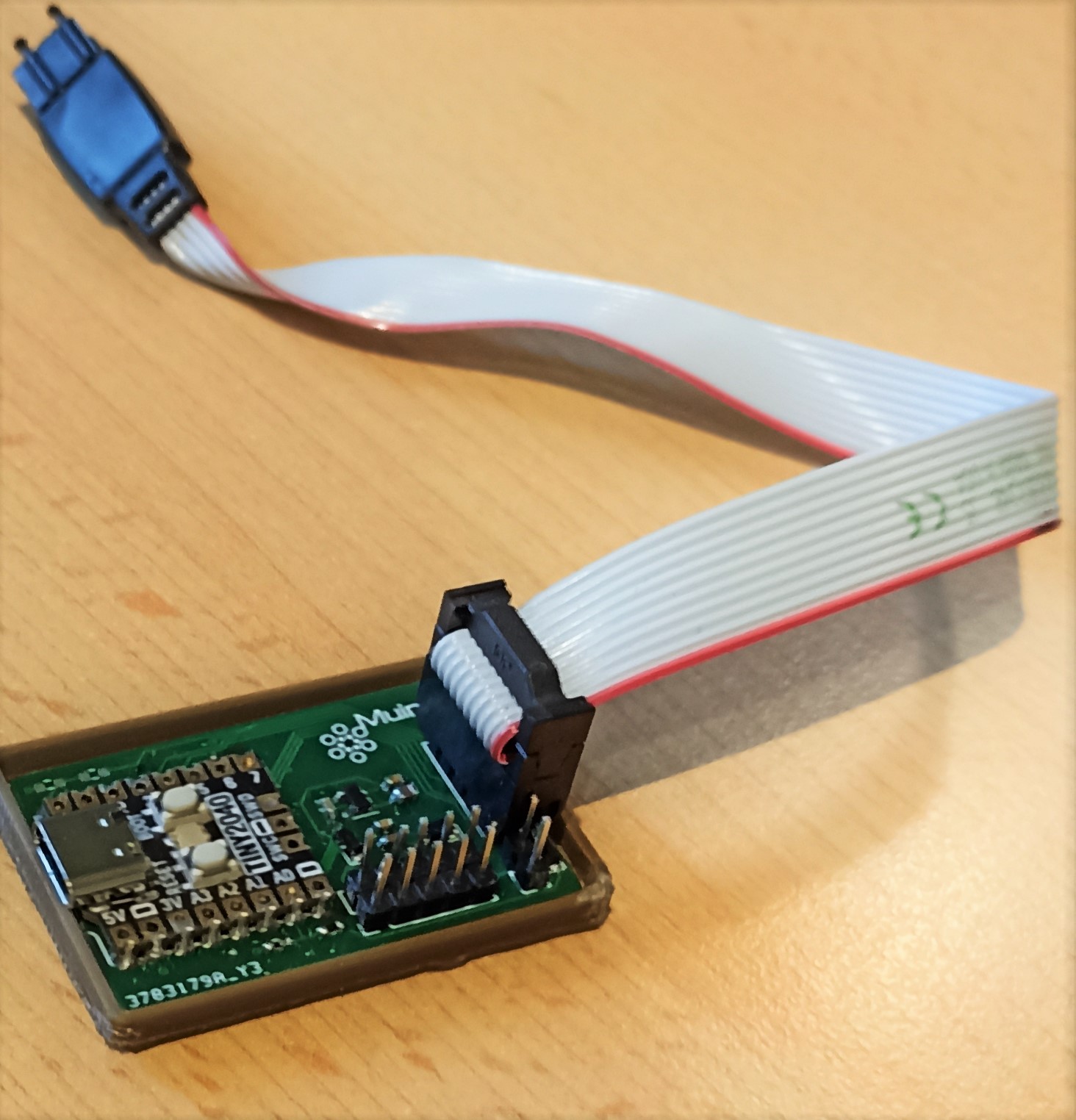
Muino debugger is an open-source printed circuit board by martijnvwezel, from the martijnvwezel/pico-probe-programmer repository on GitHub, published under the MIT licence. It is a 2-layer board of 43.2 × 27.9 mm with 18 parts on 25 nets, routed with 142 tracks and 14 vias.
Its parts include 5 capacitors, 4 resistors, 3 diodes, 3 connectors and 1 IC. It belongs with the interfaces and adapters boards and the RP2040 boards of this library.
The pico can be used to program other devices. Raspberry pi made such an effort. However there is no board yet, that is open-source and can be used with openocd as a general purpose programmer.
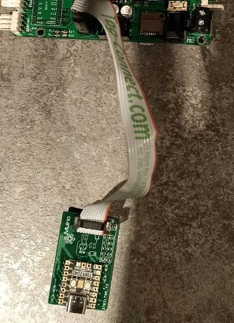
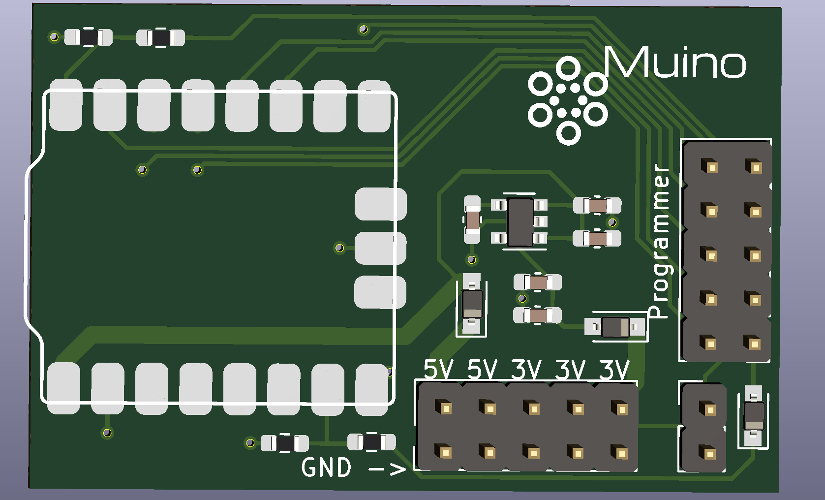
Segger Jlink bugged me because I am using a Jlink at home, and it's not compatible anymore with the newest generation of Cortex chips. Another issue that I made, I don't make them that often, but if I do I want my debugger to be able to change the pinout, like an RX, TX swap. In one of the boards, I made somehow SWO and Rx got on the wrong pin, using the pico probe I could change the location of the pins and everything worked fine :).
# Change the pins : pico-probe/src/picoprobe_config.h
# Build:
cd pico-probe
mkdir build/
cd build/
cmake ..
make -j
# Connect the picoprobe, pressing the boot button
# it shows a folder and place the file picoprobe.uf2 from the build folder
# Updated picoprobe
# for windows see docs/windows-install.md
Smalle note: the Tx 5 is not usable in this example. I didn't need it anyway.
Take a PCB maker like JLCPCB. Use the all the files from the pcb-readyto-order/, the Bom fils is not needed for that, but there is a list of the different type of components. The complete list needs to be updated soon. When I finally understand the BOM generation of Kicad. See tempory list below under Design choice chapter.
The software found in the submodules. I also added the pico-sdk to it, for code compatibility.
cd pico-probe-programmer/
git submodule update --init
Then go to the folder pico-probe, run the commands:
mkdir build/
cd build/
cmake ..
This will generate picoprobe.uf2. Or use the prebuild file: binaries/picoprobe.uf2. I prebuild this file, so I can quickly update it to a programmer if I need it again.
I like to use the Pogo style adapter. For work and hobby projects it saves a head to solder, and the PCB looks more cleaner. Sometimes I need a 3V3 power pin or 5V power pin so I added an extra header for it. If you are not interested in the 3V3 or want to save componentens? The schema part 3V3 supply does not need to be added to the pcb. Actually, the PIM558 and the programmer header are madetory. For custom program headers I added the possiblity to add 5V to pin 5 of the programmer header to disable power to the board that needs to be programmed. For my own custom boards I use the 5V to directLy power purposes.
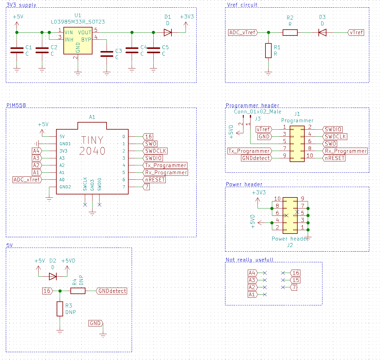
List of values, soon to be added to the schematics
In the future I want to add some extra features like read voltage of target and detection of GND. Though making it a pull-up (internally in the 2040), and read the voltage on the pin. The voltage read is what Segger-Jlinks do to detect voltage issues on target board.
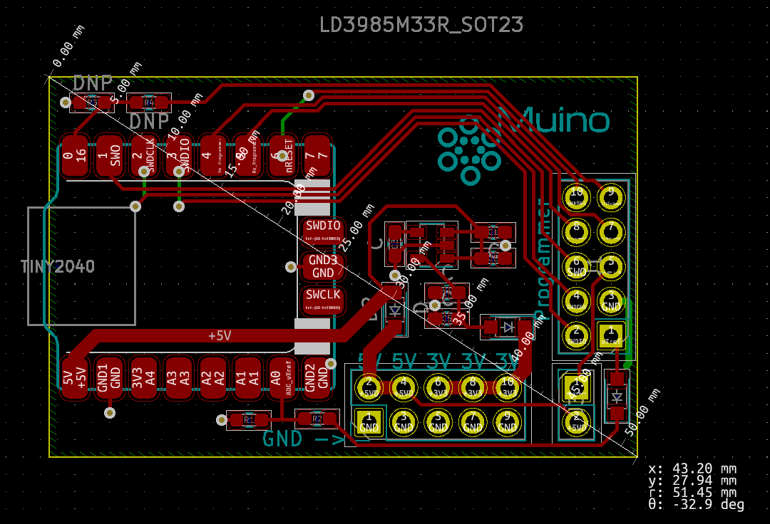
The enclosure is quickly made in Freecad with my 3D printer. I need to calibrate the heatbed again so it looks less good using my 3D printer, but it was printed in ~10min, with my help pressing down the print to the bed.
The main goal of the print was to protect the pins under the PCB.
The hardware is licensed under CERN-OHL-S v2.
| Qty | Value | Footprint | References |
|---|---|---|---|
| 5 | C | Capacitor_SMD:C_0603_1608Metric_Pad1.08x0.95mm_HandSolder | C1, C2, C3, C4, C5 |
| 3 | D | Diode_SMD:D_SOD-323_HandSoldering | D1, D2, D3 |
| 2 | DNP | Resistor_SMD:R_0603_1608Metric_Pad0.98x0.95mm_HandSolder | R3, R4 |
| 2 | R | Resistor_SMD:R_0603_1608Metric_Pad0.98x0.95mm_HandSolder | R1, R2 |
| 1 | Conn_01x02_Male | Connector_PinHeader_2.54mm:PinHeader_1x02_P2.54mm_Vertical | J3 |
| 1 | LD3985M33R_SOT23 | Package_TO_SOT_SMD:SOT-23-5 | U1 |
| 1 | LOGO | Muino_debugger:Suino | G1 |
| 1 | Power header | Connector_PinHeader_2.54mm:PinHeader_2x05_P2.54mm_Vertical | J2 |
| 1 | Programmer | Connector_PinHeader_2.54mm:PinHeader_2x05_P2.54mm_Vertical | J1 |
| 1 | TINY2040 | TINY2040:TINY2040 | A1 |
It measures 43.2 × 27.9 mm and has 2 copper layers, 1.6 mm thick.
18 parts. The full list of its parts is on this page, with links to each part's symbol and footprint where PCBKit's library has them.
From the martijnvwezel/pico-probe-programmer repository on GitHub, at the commit this page was made from: the board is pcb-kicad/Muino_debugger.kicad_pcb. PCBKit opens the board in the browser, with nothing to install.
Its repository publishes it under the MIT licence: you may reuse it on that licence's terms (keep the author's notice, and for a copyleft licence share your changes alike).

VoronDesign/Voron-Hardware
Cool Hardware designed by the Voron Design group


hackclub/OnBoard
💡 Join 1,000 teenagers and make your first PCB with a $100 grant!

VoronDesign/Voron-Tap
Tap is a nozzle-based z-probe for the V2 and Trident printer designs. The entire toolhead moves to trigger an optical switch. Tap offers many advantages:

Luos-io/luos_engine
Open-source and real-time orchestrator for cyber-physical-systems, to easily design, test and deploy embedded applications and digital twins.


Twotoz/C5VRX
Ultra-minimal, zero-CPU 5.8 GHz analog FPV video receiver using ESP32-C5 Wi-Fi 6 PHY MODEM_DIAG, BitScrambler WBFM demodulation & resistor DAC CVBS