

2 layers21 × 35 mm

 marqs85/snes_dejitter56
NES/SNES 240p de-jitter mod
Snes dejitter is an open-source printed circuit board by marqs85, from the marqs85/snes_dejitter repository on GitHub, published under the MIT licence. It is a 2-layer board of 44.1 × 23.7 mm with 39 parts on 47 nets, routed with 308 tracks and 50 vias.
It is built around the ATF1502AS-7AX44 and 2SC2412. Its parts include 14 resistors, 10 connectors, 8 capacitors, 1 IC and 1 diode. It belongs with the retro computing and games boards and the FPGA and CPLD boards of this library.
snes_dejitter is a mod board which eliminates sync jitter of NES/SNES 240p modes. Technical description and discussion is found on this thread.
Hardware
Software
Hardware
Software
NOTE: Only needed when building a custom firmware. Pre-built images can be found under output_files/ on master and nes-fix (recommended for NES/FC) branches.
Open the project file in Quartus, and run compilation
Convert MAX7000 targeted POF object file into JEDEC file suitable for 1502AS via winpof2jed.exe:
1. Select .pof file from previous step as input file
2. Select 1502AS as device
3. Change the following options:
  * Reduce MC power -> On
  * Open Collector -> Off
  * JTAG mode -> On
  * Slew rate -> Slow
4. Click "Run"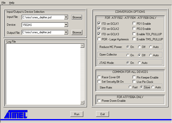
1. Create a new device chain via File->New
2. Set number of devices to 1
3. Set device to ATF1502AS
4. Set JTAG instruction to "Program/Verify"
5. Select .jed file from previous step as JEDEC file
6. Click "OK"
7. Tick "Write SVF file" and click "Run"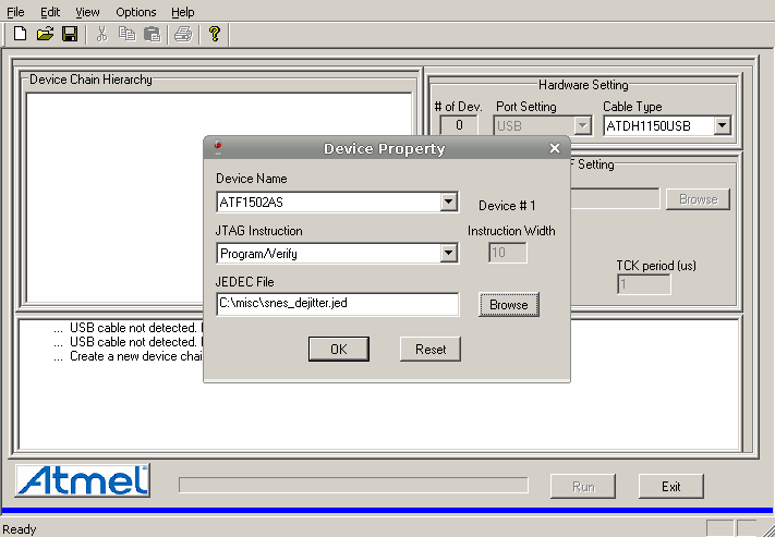
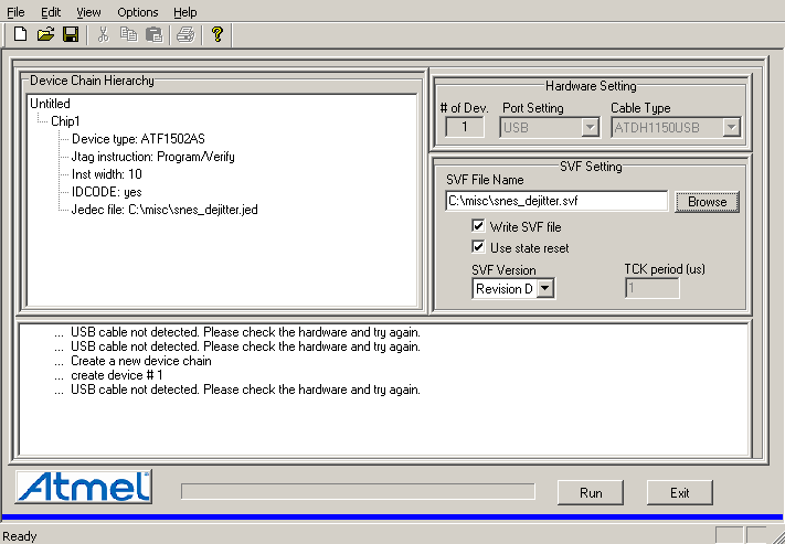
The board can be flashed using any OpenOCD supported JTAG programmer that supports 3.3V-5V IO signal level (TCK, TMS and TDI are TTL inputs with 10k pull-downs). If 3.3V IO is used, JP4 (on v1.3 PCB) should be closed which clamps TDO output to 3.3V. A standalone snes_jitter board is flashed by hooking all of its 6 JTAG header pins to respective pins of the programmer/cable, and by running flash procedure specified below. After the board has been installed to NES/SNES, firmware can be subsequently updated, but in this method 5V pin of the JTAG connector MUST be left disconnected, and programming needs to be done while NES/SNES is powered on (without a game is ok). The update procedure is similar in both cases:
| Board pin | Programmer pin |
|---|---|
| TCK | ADBUS0 |
| TMS | ADBUS3 |
| TDI | ADBUS1 |
| TDO | ADBUS2 |
openocd -f openocd.conftelnet localhost 4444
> svf <full_path_to_svf_file>General descriptions on board pins are in table below. Model-specific installation instructions are added to separate subdirectories.
| Board pin | Description |
|---|---|
| CSYNC_i | TTL C-sync signal from the console |
| MCLK_EXT_i | External clock input. Used only in PAL mode, not needed in pure NTSC installations. |
| CLK_SEL_i | Master clock source selection (0=internal/NTSC, 1=external/PAL). In PAL mode, MCLK and CSYNC are bypassed to output. Pin is pulled low internally, so it can be left disconnected in pure NTSC installations. Connected to PALMODE in multiregion installations. Can be forced high by bridging JP1 (pre-1.2 boards only), but must never be done if the pin is wired to console. |
| MCLK_o | Clock output. An optional voltage divider (R13,R14 / JP2) can be used to reduce output level from ~4Vpp to ~3Vpp, see model-specific instructions for more details. |
| CSYNC_o | C-sync output (~2.5Vpp unterminated, ~1.1Vpp into 75ohm termination) to an isolated multi-AV pin. Driver circuit is identical to SHVC-CPU-01. JP3 connects optional 330pF output capacitor that may not be present on console mainboard (not strictly needed, reduces potential noise at the price of less sharp transition time), see model-specific instructions for more details. |
| Jumper | Description |
|---|---|
| JP1 | Forces CLK_SEL_i high. Removed on v1.2 since it was mostly for debugging purposes. |
| JP2 | Enables MCLK_o voltage divider. Recommended for NES installations to ensure signal level is safe for NESRGB. |
| JP3 | Connects optional 330pF output capacitor on CSYNC_o. |
| JP4 | Enable TDO voltage clamp. Recommended if board is flashed with a 3.3V programmer. |
| Qty | Value | Footprint | References |
|---|---|---|---|
| 5 | 10k | custom_components:SM0603_Resistor_libcms | R1, R2, R3, R6, R15 |
| 4 | 0.1u | custom_components:SM0603_Capa_libcms | C2, C3, C4, C7 |
| 3 | GND | custom_components:SMD_PAD | J3, J4, J8 |
| 3 | Jumper_NO_Small | custom_components:SMD_JUMPER | JP2, JP3, JP4 |
| 2 | 12p | custom_components:SM0603_Capa_libcms | C5, C6 |
| 2 | 1k | custom_components:SM0603_Resistor_libcms | R8, R9 |
| 2 | 300 | custom_components:SM0603_Resistor_libcms | R11, R14 |
| 2 | 39 | custom_components:SM0603_Resistor_libcms | R4, R13 |
| 1 | 100 | custom_components:SM0603_Resistor_libcms | R12 |
| 1 | 10u | custom_components:SM0603_Capa_libcms | C1 |
| 1 | 1M | custom_components:SM0603_Resistor_libcms | R7 |
| 1 | 21.477272MHz | Crystals:Crystal_HC49-U_Vertical | Y1 |
| 1 | 2SC2412 | TO_SOT_Packages_SMD:SOT-23_Handsoldering | Q1 |
| 1 | 330p | custom_components:SM0603_Capa_libcms | C8 |
| 1 | 5.6k | custom_components:SM0603_Resistor_libcms | R10 |
| 1 | 5V | custom_components:SMD_PAD | J2 |
| 1 | ATF1502AS-7AX44 | custom_components:TQFP-44_10x10mm_Pitch0.8mm_Handsoldering | U1 |
| 1 | CLK_SEL_i | custom_components:SMD_PAD | J7 |
| 1 | CSYNC_i | custom_components:SMD_PAD | J5 |
| 1 | CSYNC_o | custom_components:SMD_PAD | J10 |
| 1 | JTAG_CONN | custom_components:JTAG_Header_Angled_1x06_Pitch2.54mm | J1 |
| 1 | MCLK_EXT_i | custom_components:SMD_PAD | J6 |
| 1 | MCLK_o | custom_components:SMD_PAD | J9 |
| 1 | Zener_3v3 | custom_components:SOD-323_Handsoldering | D1 |

whitequark/ATF15xx-EVB
Cheap & simple evaluation boards for Microchip ATF15xx CPLDs

joeycastillo/Sensor-Watch
A board replacement for the classic Casio F-91W wristwatch

rusefi/rusefi
rusefi - GPL internal combustion engine control unit

hackclub/OnBoard
💡 Join 1,000 teenagers and make your first PCB with a $100 grant!

ataradov/usb-sniffer-lite
A simple USB sniffer based on Raspberry Pi RP2040

windowsair/wireless-esp8266-dap
CMSIS-DAP compatible wireless debugger for ESP8266/ESP32/ESP32C3/ESP32S3. Optional 40MHz SPI acceleration, etc. 适配多种ESP芯片的无线调试器

It measures 44.1 × 23.7 mm and has 2 copper layers, 1.6 mm thick.
39 parts, built around the ATF1502AS-7AX44 and 2SC2412. The full list of its parts is on this page, with links to each part's symbol and footprint where PCBKit's library has them.
From the marqs85/snes_dejitter repository on GitHub, at the commit this page was made from: the board is pcb/snes_dejitter.kicad_pcb. PCBKit opens the board in the browser, with nothing to install.
Its repository publishes it under the MIT licence: you may reuse it on that licence's terms (keep the author's notice, and for a copyleft licence share your changes alike).