4 layers29 × 31.7 mm
ESP32-C3-mini
max-bispham/esp32-module-board-tutorial
Tutorial design I followed in order to learn kicad, pcb design process and schematic layout
29 parts

 marouane-daoudi/esp32-c3-dev-board
4-layer ESP32-C3 WROOM development board with USB-C, ESD protection, LDO regulation and differential pair routing — designed in KiCad
ESP32 C3 Mini is an open-source printed circuit board by marouane-daoudi, from the marouane-daoudi/esp32-c3-dev-board repository on GitHub. It is a 4-layer board of 32.6 × 40 mm with 31 parts on 30 nets, routed with 164 tracks and 32 vias.
It is built around the ESP32-C3-WROOM-02-H4, AP2112K-3.3 and USBLC6-2P6, with the PESD5V0L1UL among its other parts. Its parts include 10 capacitors, 10 resistors, 3 ICs, 3 connectors and 2 diodes. It belongs with the ESP32 and RISC-V boards of this library.


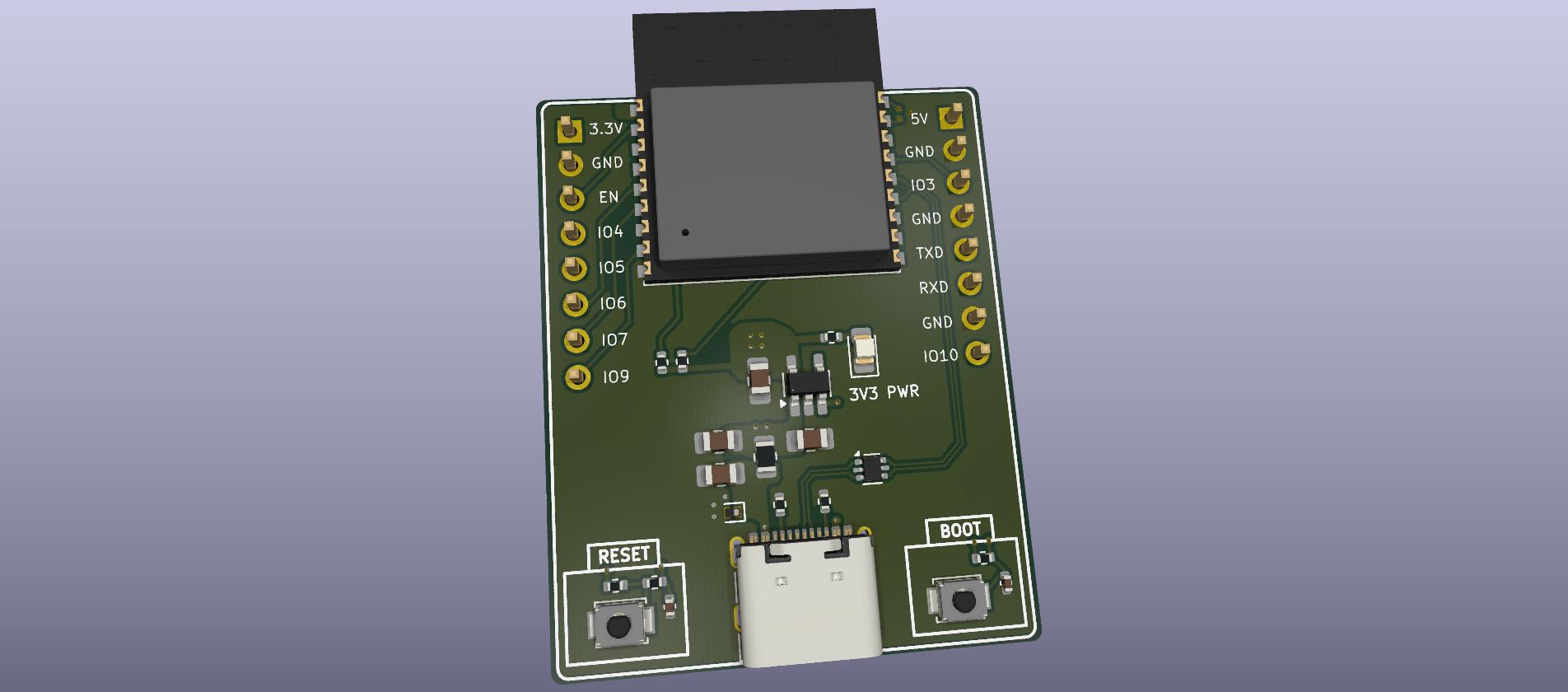
A 4-layer development and testing board for the ESP32-C3-WROOM-02 module. It uses USB-C for 5V input and USB 2.0 data, includes onboard 3.3V LDO regulation, ESD protection on the USB data and VBUS lines, an external crystal, reset and boot buttons, a 3.3V power indicator LED, and breadboard-compatible GPIO headers.
The board was designed in KiCad 10.0 with a focus on power integrity, signal routing, ESD return paths, and low-impedance power distribution.
| Parameter | Value |
|---|---|
| Target module | ESP32-C3 WROOM-02 |
| PCB layers | 4-layer FR4 |
| Board width | 27.94mm (breadboard compatible) |
| Pin pitch | 2.54mm |
| Input | 5V via USB-C |
| Regulated output | 3.3V — AP2112K-3.3TRG1 LDO (600mA max) |
| ESD protection (data) | USBLC6-2SC6 dual ESD diode |
| ESD protection (VBUS) | PESD5V0L1UL |
| Crystal | External oscillator for USB timing |
| Power indicator | Green LED (NATIONSTAR NCD0805G1) |
| Design tool | KiCad |
| Left Header | Right Header |
|---|---|
| 3.3V | 5V |
| GND | GND |
| EN | IO3 |
| IO4 | GND |
| IO5 | TXD |
| IO6 | RXD |
| IO7 | GND |
| IO9 | IO10 |
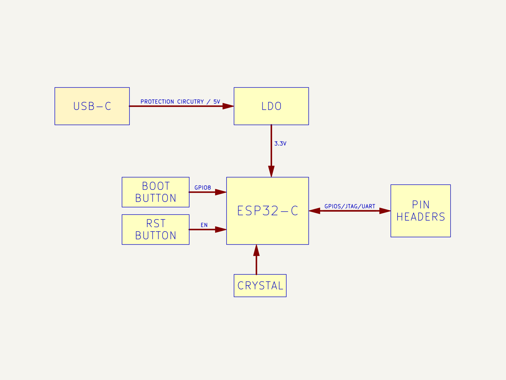
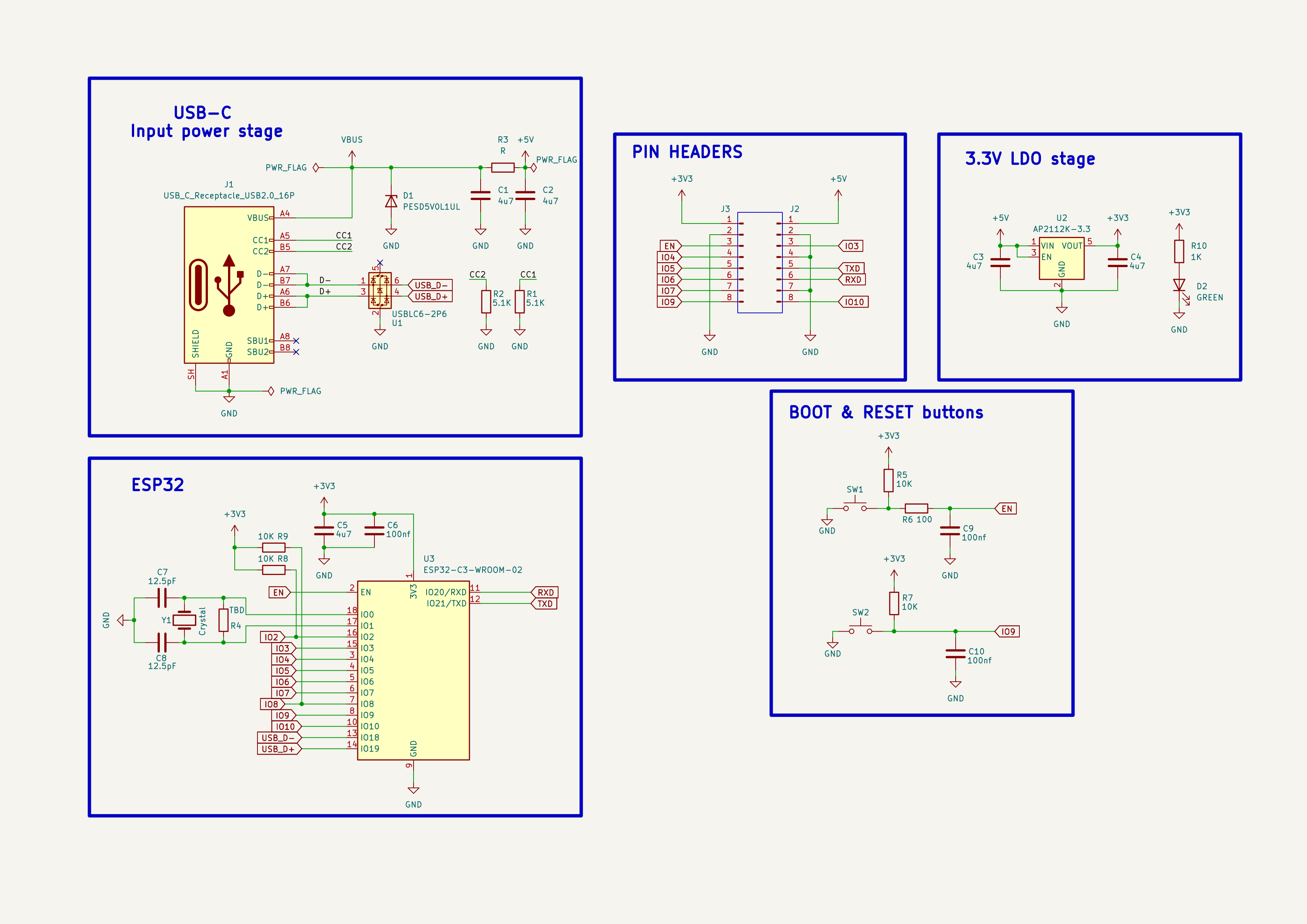
A 16-pin USB-C receptacle provides 5V input power and USB 2.0 data. Three groups of pins are used:
CC1 and CC2 — each connected to GND through a 5.1kΩ resistor. These configuration channel pins tell the upstream power source that this board is a power sink requesting 5V at standard current. Without these resistors, modern USB-C chargers and laptop ports will not supply power. Both pins require their own resistor because the cable can be inserted in either orientation — only one CC pin is active per insertion but both must be terminated.
D+ and D- — USB 2.0 data lines connected to the ESP32-C3 through the USBLC6-2SC6 dual ESD protection IC. This device was chosen for its low line capacitance, which is critical for preserving signal integrity on high-speed differential pairs — excessive capacitance loads the lines and degrades eye diagrams at USB Full Speed. A single IC protects both lines simultaneously.
VBUS — the 5V supply rail, protected and filtered before entering the rest of the circuit through two stages: a PESD5V0L1UL ESD diode clamping surge voltages, followed by a pi filter (capacitor — 0Ω resistor — capacitor) for additional conducted noise filtering. The 0Ω resistor is a deliberate design choice — it can be replaced with a polyfuse for overcurrent protection on future revisions without redesigning the PCB.
The AP2112K-3.3TRG1 LDO regulates 5V from VBUS down to the 3.3V required by the ESP32-C3. It was chosen over a switching regulator for two reasons: it keeps the design compact, and it produces no switching noise — important for a board with RF and ADC functionality where a switching regulator's ripple could degrade performance.
The AP2112K is rated for 600mA output current, covering the ESP32-C3's typical current demand with sufficient margin. The datasheet recommends 1µF input and output decoupling capacitors. 4.7µF was used instead for two reasons: the same value was already introduced in the pi filter stage (simplifying the BOM), and slightly larger decoupling capacitance improves transient response under sudden load steps.
An external crystal oscillator provides the precise clock reference required for USB Full Speed timing. The ESP32-C3 WROOM module includes an internal RC oscillator but it is insufficiently accurate for USB — USB 2.0 Full Speed requires clock accuracy within ±2500ppm, which only an external crystal can reliably provide. Load capacitors are placed symmetrically on both crystal pins per the datasheet recommendations.
A push button pulls the EN pin to GND when pressed, triggering a hard reset of the ESP32-C3. EN is normally held HIGH through a pull-up resistor to VCC. An RC filter is added per the ESP32-C3 datasheet recommendation — the resistor and capacitor form a low-pass filter that prevents mechanical switch bounce from generating spurious reset pulses. Without this filter, a single physical button press can produce multiple rapid transitions on EN, causing repeated resets instead of a clean single reset event.
The ESP32-C3 determines boot mode by reading IO2, IO8, and IO9 at startup. For normal operation all three must be HIGH. For USB download mode (firmware flashing), IO9 must be LOW while the others remain HIGH. IO2 and IO8 are permanently pulled HIGH through resistors. A dedicated BOOT button pulls IO9 LOW only when pressed — releasing it returns IO9 HIGH through its pull-up resistor, allowing normal operation. The button is only effective when pressed simultaneously with RESET, which forces the chip to sample the boot pins at startup.
A green LED (NATIONSTAR NCD0805G1, 0805 package) with a 1kΩ current-limiting resistor indicates active 3.3V power on the board. It was added after the rest of the design was complete as a simple functional indicator.
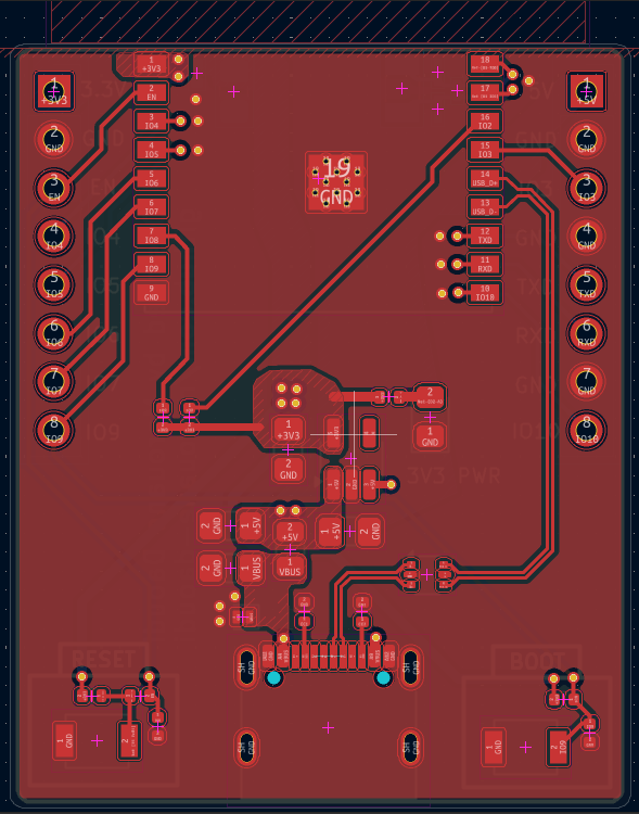
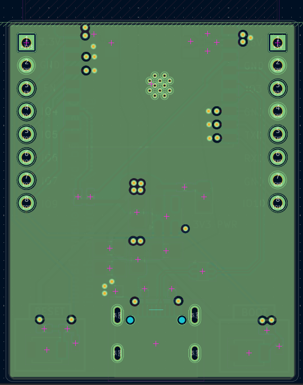
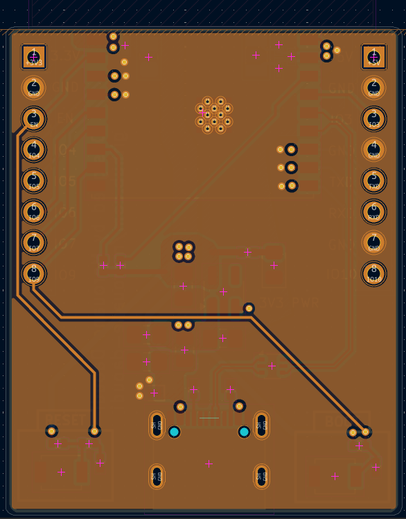
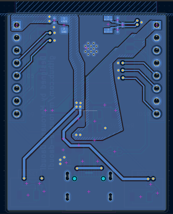
| Layer | Function |
|---|---|
| Layer 1 (top) | Signal routing, components, ESD, LDO, USB-C |
| Layer 2 | Continuous solid ground plane |
| Layer 3 | Long switch connections (EN and IO9 routing only) |
| Layer 4 (bottom) | Power distribution planes (VBUS, 3.3V), crystal, additional signals |
Layer 2 is kept as an uninterrupted solid ground plane throughout the entire board. Every high-speed signal on the top layer is referenced to this plane, ensuring a controlled return path directly beneath each trace. This is the single most important layout decision on the board — a broken ground plane forces return currents to take longer paths, increasing loop inductance and radiating EMI.
Components were placed by following the power flow of the circuit from input to output, grouping by functional block before routing began:
USB-C connector at the bottom edge → ESD protection immediately adjacent → pi filter following → LDO stage → decoupling capacitors → ESP32-C3 module at the top. This left-to-right, input-to-output placement minimizes trace length on the power path and keeps high-current paths short and direct.
All power connections use custom-shaped local copper planes rather than routed traces. Three separate planes were defined: one for VBUS (5V from USB), one for the LDO input (5V filtered), and one for the 3.3V output. Copper planes provide significantly lower resistance and inductance than traces of equivalent length — critical during transient load events when the ESP32-C3 core suddenly demands current during Wi-Fi transmission bursts.
The 3.3V plane runs from the LDO output capacitor directly to the ESP32-C3 decoupling capacitors, ordered deliberately: the 4.7µF bulk capacitor sees the current first, followed by the 100nF high-frequency decoupling capacitor, then vias transfer the 3.3V to the ESP32-C3 power pin on the front layer. THT pin headers connect directly to the back copper plane, providing clean 3.3V and 5V access at the headers without additional routing.
The USBLC6-2SC6 (data line ESD) and PESD5V0L1UL (VBUS ESD) are placed immediately at the USB-C connector pads — the first components the external signals reach after entering the board. Three ground vias are placed directly adjacent to the ESD diode ground pads, providing the shortest possible low-impedance discharge path to the ground plane during an ESD event. Inductance in the discharge path reduces clamping effectiveness — minimizing this path length is as important as the protection device selection itself.
D+ and D- are routed as a tightly coupled differential pair on the top layer, referenced to the continuous ground plane on layer 2. The route is kept short from the USB-C connector through the ESD protection device to the ESP32-C3 module. Trace spacing is kept consistent and the pair is routed with USB impedance control in mind. Routing on the surface layer directly above the ground plane ensures a well-defined return path with minimal loop area.
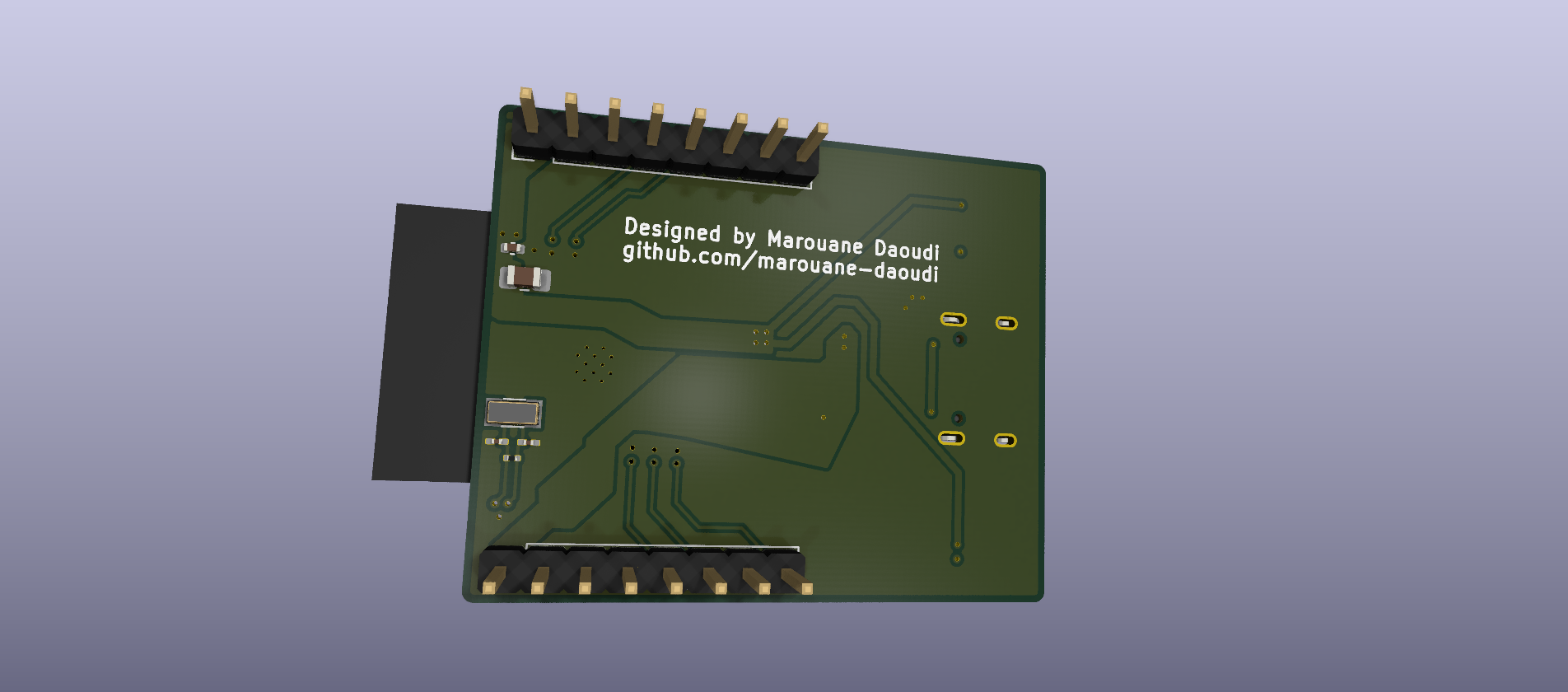
The crystal and its load capacitors are placed on the back layer to conserve space on the front. Traces are kept short and routed symmetrically on both oscillator pins — asymmetry in crystal routing introduces parasitic differences between the two pins that can prevent oscillation startup or cause frequency instability. Vias transfer the crystal signals between back and front layers at the ESP32-C3 pins.
GPIO and power pins for the headers were routed straightforwardly. Where traces would have conflicted with high-speed signal areas on the front layer, the THT nature of the pin headers was exploited — signals were dropped to the back layer via vias and routed there, keeping the top layer clean for the differential pair and crystal signals. The EN and IO9 connections to the RESET and BOOT buttons required a long connection routed on layer 3 to avoid interference with other routing layers.
Ground copper fills were applied to all four layers after routing was complete, filling all unused copper areas. This reduces EMI by eliminating antenna-like copper islands, lowers ground impedance across the board, and provides additional shielding between signal layers. Layer 2 was maintained as a completely uninterrupted solid ground plane with no signal routing passing through it at any point.
A 5mm keep-out zone is enforced beneath the ESP32-C3 WROOM module's PCB antenna on all four layers. Copper beneath the antenna detunes it by altering the antenna's electromagnetic environment, reducing Wi-Fi range and reliability. No traces, planes, or fills enter this zone.
This was the most technically demanding board in this portfolio and introduced concepts not present in simpler 2-layer designs:
Gerber files in /gerbers verified with JLCPCB's online
Gerber viewer.
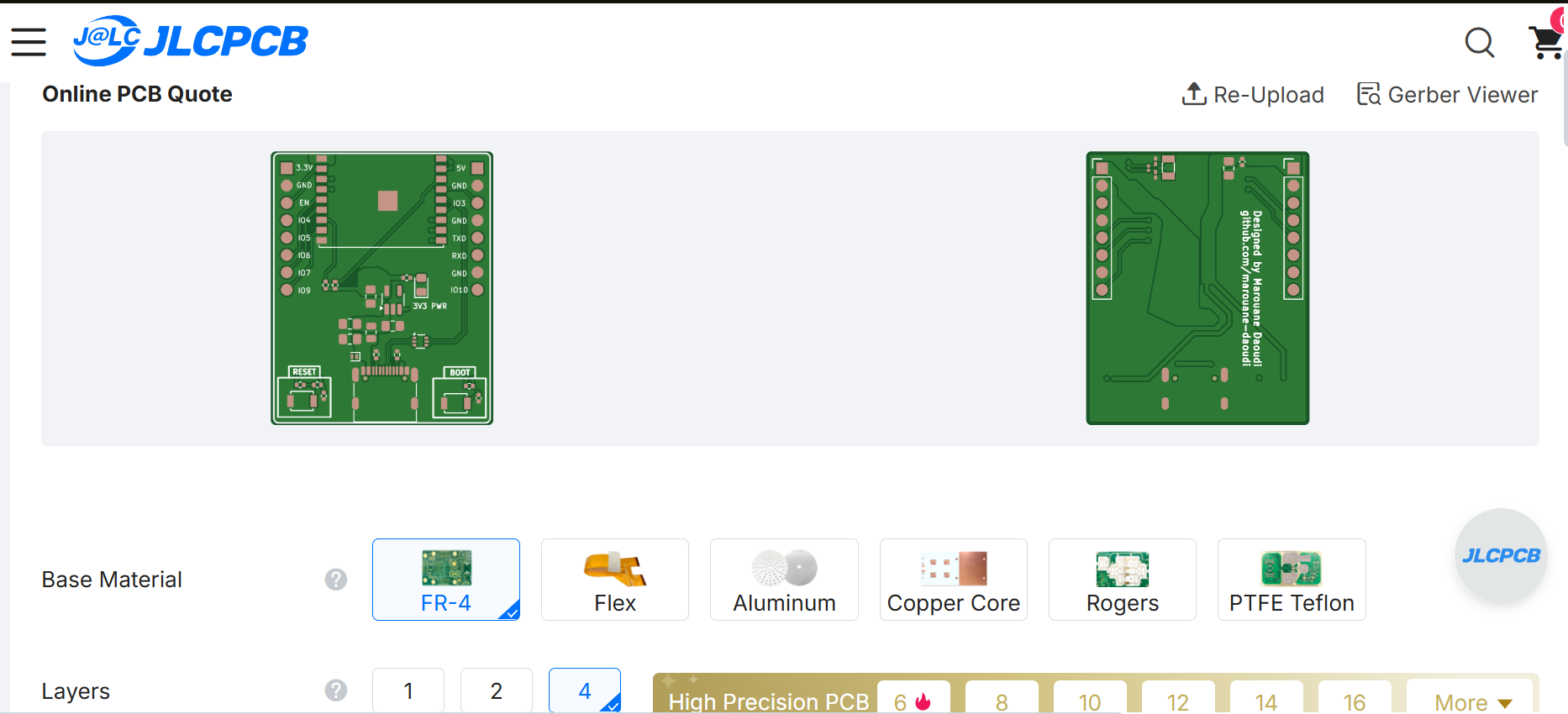
To order, zip the contents of the gerbers folder and upload to JLCPCB or PCBWay. Select:
| Folder | Contents |
|---|---|
/kicad | Schematic, PCB, and KiCad project files |
/gerbers | Fabrication-ready Gerber and drill files |
/images | 3D renders, PCB layer screenshots, schematic images, and Gerber previews |
Circuit design and PCB layout process based on the tutorial Design a Custom ESP32-Mini Board in KiCad 9 by [PajoPCB]. No source files were provided in the original video — schematic, PCB layout, component selection, and all KiCad files in this repository were built independently while following the tutorial's design approach.
Marouane Daoudi
Electrical Engineering student
Designed in KiCad
| Qty | Value | Footprint | References |
|---|---|---|---|
| 5 | 4u7 | Capacitor_SMD:C_0805_2012Metric_Pad1.18x1.45mm_HandSolder | C1, C2, C3, C4, C5 |
| 4 | 10K | Resistor_SMD:R_0402_1005Metric | R5, R7, R8, R9 |
| 3 | 100nf | Capacitor_SMD:C_0402_1005Metric | C6, C9, C10 |
| 2 | 12.5pF | Capacitor_SMD:C_0201_0603Metric_Pad0.64x0.40mm_HandSolder | C7, C8 |
| 2 | 5.1K | Resistor_SMD:R_0402_1005Metric | R1, R2 |
| 2 | Conn_01x08_Pin | Connector_PinHeader_2.54mm:PinHeader_1x08_P2.54mm_Vertical | J2, J3 |
| 2 | SW_Push | Button_Switch_SMD:SW_SPST_B3U-1000P | SW1, SW2 |
| 1 | 100 | Resistor_SMD:R_0402_1005Metric | R6 |
| 1 | 1K | Resistor_SMD:R_0402_1005Metric | R10 |
| 1 | AP2112K-3.3 | Package_TO_SOT_SMD:SOT-23-5_HandSoldering | U2 |
| 1 | Crystal | Crystal:Crystal_SMD_3215-2Pin_3.2x1.5mm | Y1 |
| 1 | ESP32-C3-WROOM-02 | RF_Module:ESP32-C3-WROOM-02 | U3 |
| 1 | GREEN | LED_SMD:LED_0805_2012Metric_Pad1.15x1.40mm_HandSolder | D2 |
| 1 | PESD5V0L1UL | Diode_SMD:D_SOD-882 | D1 |
| 1 | R | Resistor_SMD:R_0805_2012Metric | R3 |
| 1 | TBD | Resistor_SMD:R_0201_0603Metric | R4 |
| 1 | USBLC6-2P6 | Package_TO_SOT_SMD:SOT-666 | U1 |
| 1 | USB_C_Receptacle_USB2.0_16P | Connector_USB:USB_C_Receptacle_G-Switch_GT-USB-7010ASV | J1 |
max-bispham/esp32-module-board-tutorial
Tutorial design I followed in order to learn kicad, pcb design process and schematic layout

Srushti-D-Hebbar/esp32-c3-wroom02-development-board
A custom 4-layer ESP32-C3-WROOM-02 development board designed in KiCad 10 - includes USB-C power/data, schematics, PCB layout, and manufacturing files.

Supriya648/ESP32-S3-XR-Glasses-PCB
Custom PCB with ESP32-S3 camera module for AI/XR glasses

akashh218/ESP32-CAM-Devlopment-board
Custom 4-layer ESP32-S3 camera development board designed in KiCad, featuring camera and microSD interfaces, dual USB-C connectivity, UART programming, GPIO expansion, power management, and RF-aware PCB layout.

JoshAyersSBT/Robot_Arm_PCB
This document consolidates the power architecture, wiring, BOM additions, and system diagram for an ESP32-based robot arm controller using:


IvanVeloz/smart-usb-plug
A smart plug for USB with energy measurement and Matter over Thread support

21shravan/AT89s51-dev-board
A modern AT89S52 (8051) development board featuring USB Type-C power, CH340C USB-to-UART, ISP programming, and a complete open-source hardware design documented from schematic to PCB.
It measures 32.6 × 40 mm and has 4 copper layers, 1 mm thick.
31 parts, built around the ESP32-C3-WROOM-02-H4, AP2112K-3.3, USBLC6-2P6 and PESD5V0L1UL. The full list of its parts is on this page, with links to each part's symbol and footprint where PCBKit's library has them.
From the marouane-daoudi/esp32-c3-dev-board repository on GitHub, at the commit this page was made from: the board is kicad/ESP32_C3_Mini.kicad_pcb and its schematic kicad/Block_diagram.kicad_sch. PCBKit opens the board in the browser, with nothing to install.
Its repository states no licence, so its author keeps all rights: ask marouane-daoudi before reusing the design.