Skip to the content
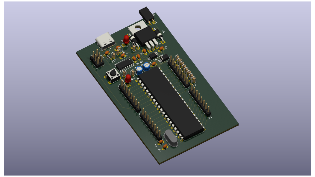
2 layers54.5 × 90 mmDev board, the printed circuit board in 3D

A modern AT89S52 (8051) development board featuring USB Type-C power, CH340C USB-to-UART, ISP programming, and a complete open-source hardware design documented from schematic to PCB.

Size
54.5 × 90 mm
Copper layers
2
Thickness
1.6 mm
Parts
44
Nets
64
Pads
194
Tracks, vias
339, 23
Pours
2
Routed
Yes
KiCad
KiCad 9.0 (file 20241229)
Created
28 Jun 2026
Updated
4 Jul 2026

Overview

Dev board is an open-source printed circuit board by 21shravan, from the 21shravan/AT89s51-dev-board repository on GitHub. It is a 2-layer board of 54.5 × 90 mm with 44 parts on 64 nets, routed with 339 tracks and 23 vias.

It is built around the CH340C, SS14 and PESD5V0L1UL. Its parts include 13 resistors, 12 capacitors, 7 diodes, 7 connectors and 3 ICs. It belongs with the microcontroller boards boards and the 8051 (CH55x, STC, AT89) boards of this library.

Main components

3

README

README.md

AT89s51-dev-board

A modern AT89S52 (8051) development board featuring USB Type-C power, CH340C USB-to-UART, ISP programming, and a complete open-source hardware design documented from schematic to PCB.

Overview

This project aims to build a modern development board around the AT89S52 microcontroller with features commonly found in commercial development boards while keeping the design simple, educational, and open-source.

Unlike many existing AT89S52 boards, this design integrates USB Type-C power, USB-to-UART communication, and ISP programming support, making it more convenient for modern development.


Preview

PCB 3D Render


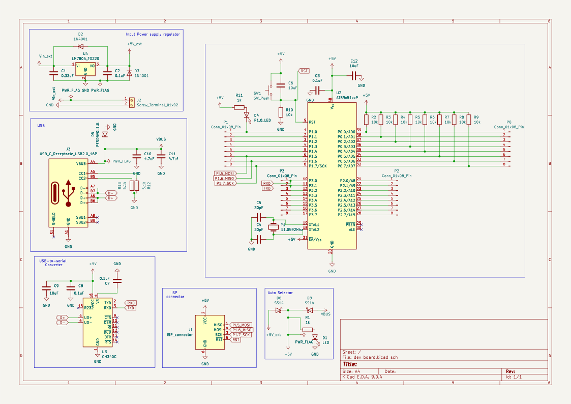
Schematic


Features

  • AT89S51 (8051 Architecture)
  • USB Type-C Power Input
  • CH340C USB-to-UART Converter
  • Automatic Power Source Selection
  • External Power Input
  • ISP Programming Header
  • 11.0592 MHz Crystal Oscillator
  • Hardware Reset Circuit
  • Power LED
  • GPIO Expansion Headers
  • 5V Logic

Block Diagram

text
                    +--------------------+
                    |     USB Type-C     |
                    +---------+----------+
                              |
                    +---------v----------+
                    | Power Protection   |
                    | & Auto Selection   |
                    +---------+----------+
                              |
                            +5V Rail
                              |
      +-----------------------+-----------------------+
      |                                               |
+-----v------+                               +--------v--------+
|   CH340C   |                               |    AT89S52      |
| USB-UART   |<-------- UART --------------->| 8051 MCU        |
+------------+                               +--------+--------+
                                                      |
                                        +-------------+-------------+
                                        |                           |
                                   ISP Header                 GPIO Headers

Power Architecture

The board supports two power sources:

  • USB Type-C (5V)
  • External 5V Supply

Automatic source selection is implemented using Schottky diode OR-ing to prevent reverse current between the two supplies.


USB Interface

The onboard CH340C provides:

  • USB-to-UART communication
  • Serial debugging
  • Terminal communication

Note: The CH340C cannot program the AT89S52. Programming is performed through the ISP header.


Programming

Programming is performed using an external ISP programmer.

Supported programmers include:

  • USBasp
  • AT89 ISP Programmer
  • Compatible 8051 ISP programmers

Planned Features

  • USB ESD Protection
  • Resettable Polyfuse
  • User LEDs
  • Push Buttons
  • LCD Header
  • Buzzer
  • Servo Header
  • 3.3V Output
  • Test Points
  • Silkscreen Labels

Design Tools

  • KiCad
  • Proteus (Firmware Testing)
  • Keil µVision (Firmware Development)

Objectives

This project is being developed to:

  • Practice professional PCB design
  • Learn USB Type-C implementation
  • Understand power management techniques
  • Design reliable embedded hardware
  • Create an open-source AT89S51 development platform

Future Improvements

  • Native USB Programmer
  • On-board Bootloader
  • SWD/JTAG Debug Interface (for future MCU variants)
  • Modular Expansion System
  • Integrated Logic Analyzer Header

Author

Shravan Mathapati


Contributing

Suggestions, improvements, and pull requests are always welcome.

If you find any issues with the schematic or PCB, feel free to open an issue or submit a pull request.


⭐ If you find this project useful, consider giving it a star!

Parts

44
QtyValueFootprintReferences
910kResistor_THT:R_Axial_DIN0204_L3.6mm_D1.6mm_P1.90mm_VerticalR2, R3, R4, R5, R6, R7, R8, R9, R10
40.1uFCapacitor_THT:C_Disc_D3.0mm_W1.6mm_P2.50mmC2, C3, C7, C8
4Conn_01x08_PinConnector_PinHeader_2.54mm:PinHeader_1x08_P2.54mm_VerticalP0, P1, P2, P3
210uFCapacitor_THT:CP_Radial_D4.0mm_P1.50mmC6, C12
21N4001Diode_THT:D_DO-41_SOD81_P10.16mm_HorizontalD2, D3
21kResistor_THT:R_Axial_DIN0204_L3.6mm_D1.6mm_P1.90mm_VerticalR1, R11
230pFCapacitor_THT:C_Disc_D3.0mm_W1.6mm_P2.50mmC4, C5
25.1kResistor_THT:R_Axial_DIN0204_L3.6mm_D1.6mm_P1.90mm_VerticalR12, R13
2SS14Diode_SMD:D_SMAD6, D8
10.33uFCapacitor_THT:C_Disc_D3.0mm_W1.6mm_P2.50mmC1
110uFCapacitor_THT:C_Disc_D3.0mm_W1.6mm_P2.50mmC9
111.0592MhzCrystal:Crystal_HC49-4H_VerticalY1
14.7uFCapacitor_THT:C_Disc_D3.0mm_W1.6mm_P2.50mmC10
14.7ufCapacitor_THT:C_Disc_D3.0mm_W1.6mm_P2.50mmC11
1AT89x51xxPPackage_DIP:DIP-40_W15.24mmU2
1CH340CPackage_SO:SOIC-16_3.9x9.9mm_P1.27mmU3
1ISP_connectorConnector_PinHeader_2.54mm:PinHeader_2x03_P2.54mm_VerticalJ1
1LEDLED_THT:LED_D3.0mmD1
1LM7805_TO220Package_TO_SOT_THT:TO-220-3_Horizontal_TabDownU4
1P1.0_LEDLED_THT:LED_D3.0mmD4
1PESD5V0L1ULDiode_SMD:D_SOD-882D5
1SW_PushButton_Switch_THT:SW_PUSH_6mm_H5mmSW1
1Screw_Terminal_01x02Connector_PinSocket_2.54mm:PinSocket_1x02_P2.54mm_HorizontalJ2
1USB_C_Receptacle_USB2.0_16PConnector_USB:USB_C_Receptacle_GCT_USB4105-xx-A_16P_TopMnt_HorizontalJ3

Similar boards

  • 4 layers60 × 80 mmWisp, the printed circuit board in 3D

    Wisp

    huulanka/wisp

    Open-source ESP32 room climate monitor — CO2, VOC, humidity, temperature and light sensing with custom PCB, MQTT/HomeKit integration, and OTA firmware updates. Full hardware + software, from schematic to BOM.

    91 partsMIT
  • 2 layers110.7 × 109.2 mmESP32S3R8 XR GL, the printed circuit board in 3D

    ESP32S3R8 XR GL

    Supriya648/ESP32-S3-XR-Glasses-PCB

    Custom PCB with ESP32-S3 camera module for AI/XR glasses

    80 parts
  • 4 layers79.5 × 20 mmMatter usb switch, the printed circuit board in 3D

    Matter usb switch

    IvanVeloz/smart-usb-plug

    A smart plug for USB with energy measurement and Matter over Thread support

    65 parts2GPL-3.0
  • 4 layers72.6 × 35.8 mmEsp32 cam, the printed circuit board in 3D

    Esp32 cam

    akashh218/ESP32-CAM-Devlopment-board

    Custom 4-layer ESP32-S3 camera development board designed in KiCad, featuring camera and microSD interfaces, dual USB-C connectivity, UART programming, GPIO expansion, power management, and RF-aware PCB layout.

    54 parts
  • 2 layers46 × 26.8 mmVga breakout, the printed circuit board in 3D

    Vga breakout

    DinE-1/vgaBreakoutBoard

    A KiCad PCB breakout board providing easy access to VGA connector pins.

    14 partsCERN-OHL-P-2.0
  • 4 layers100 × 100 mmTankervision pdb, the printed circuit board in 3D

    Tankervision pdb

    ikeefe12/tankervision-pdb

    Four-layer KiCad power distribution board for the TankerVision robot: USB-C PD / barrel-jack input, supercapacitor-backed rail for clean Jetson shutdown, and four firmware-controlled protected output ports.

    452 parts
  • 4 layers29.7 × 28.5 mmHdmi injector, the printed circuit board in 3D

    Hdmi injector

    JaydenN117/i2C-HDMI-injector

    Injects i2c signal to Dasung Paperlike Pro monitor through HDMI.

    20 partsMIT
  • 2 layersRobot Arm PCB, the printed circuit board in 3D

    Robot Arm PCB

    JoshAyersSBT/Robot_Arm_PCB

    This document consolidates the power architecture, wiring, BOM additions, and system diagram for an ESP32-based robot arm controller using:

    26 parts

Questions

How big is the Dev board PCB?

It measures 54.5 × 90 mm and has 2 copper layers, 1.6 mm thick.

What parts does the Dev board use?

44 parts, built around the CH340C, SS14 and PESD5V0L1UL. The full list of its parts is on this page, with links to each part's symbol and footprint where PCBKit's library has them.

Where can I download the Dev board KiCad files?

From the 21shravan/AT89s51-dev-board repository on GitHub, at the commit this page was made from: the board is dev_board.kicad_pcb and its schematic dev_board.kicad_sch. PCBKit opens the board in the browser, with nothing to install.

Can I use the Dev board design in my own project?

Its repository states no licence, so its author keeps all rights: ask 21shravan before reusing the design.