
2 layers
 markusgruen/DccFunctionDecoder3
Open source, Arduino-based DCC function decoder
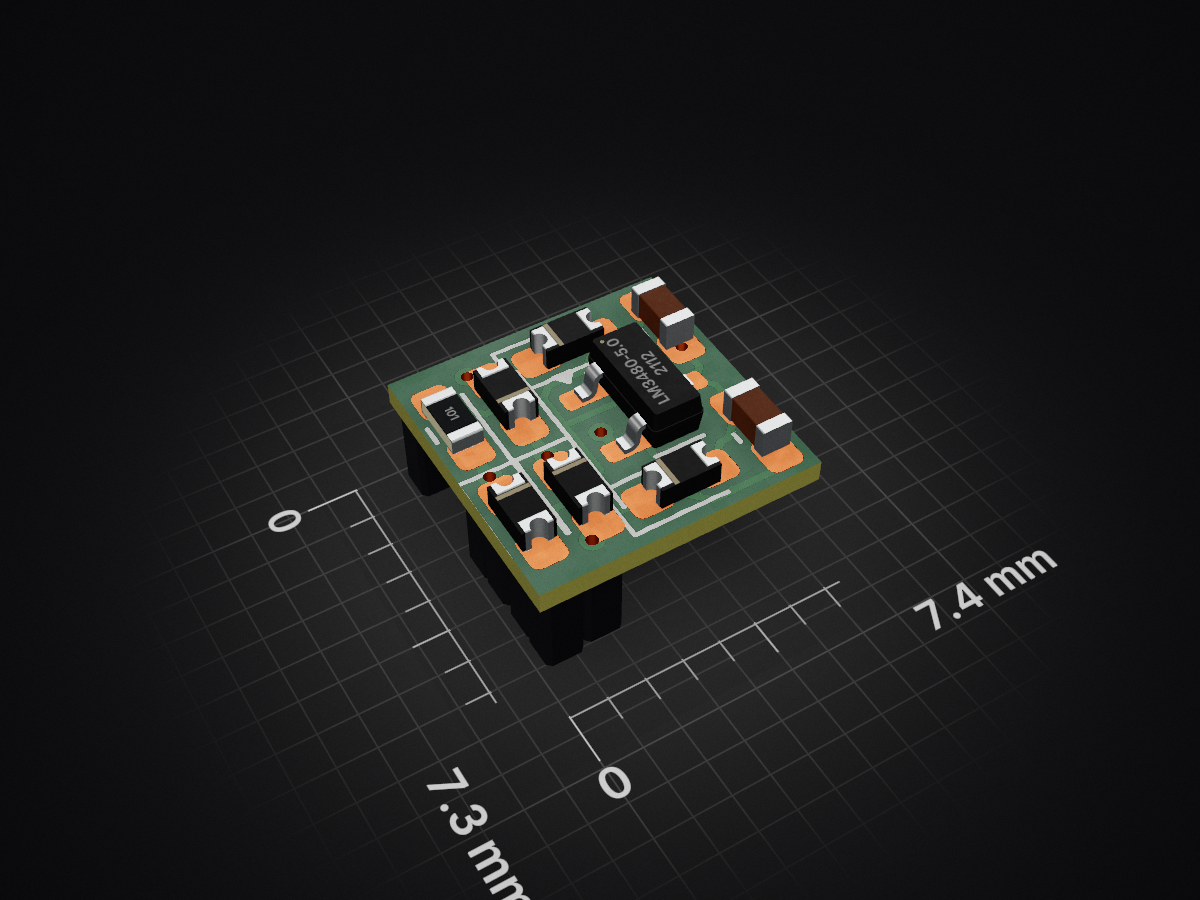
DCC Dekoder Attiny402 1 is an open-source printed circuit board by markusgruen, from the markusgruen/DccFunctionDecoder repository on GitHub, published under the GPL-3.0 licence. It is a 2-layer board of 7.4 × 7.3 mm with 17 parts on 12 nets, routed with 68 tracks and 7 vias.
It is built around the ATTINY402-SSN. Its parts include 6 connectors, 5 diodes, 2 capacitors, 2 resistors and 2 ICs. It belongs with the AVR (ATmega, ATtiny) boards of this library.
Hier klicken für deutsch: Deutsche Doku
A simple DCC function decoder with 4 AUX channels. Compiles for an ATtiny402
Functionality:
KiCad files are available in the Hardware-folder
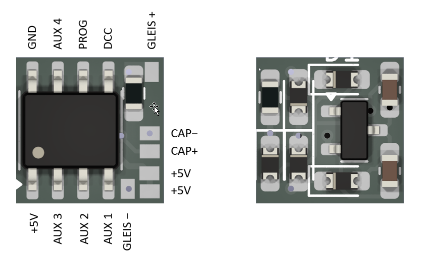
The PCB has a size of approx. 7 by 7 mm. PCB is double-sided and only has standard components in the size of 0603 or larger to enable hand soldering of the decoder.
The software can be compiled and flashed using the Arduino environment.
You will require a standard USB-UART adapter (5V compatible). Connect the adapter as shown with the decoder. You MUST NOT connect the decoder's 5V with the UART-adapter. The LDO on the decoder does not like being reverse powered. Switch on the rail's power supply.
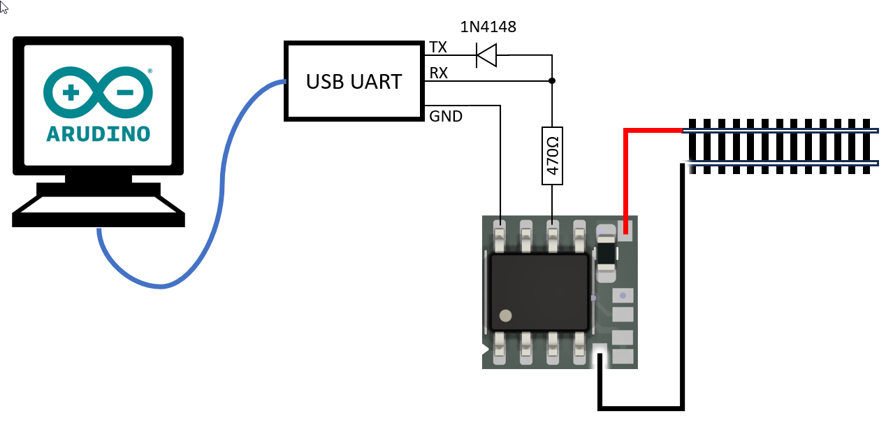
Select the appropriate COM port in the Arduino IDE and select Sketch -> Upload using Programmer (or hit CTRL+SHIFT+U). Just hitting the Upload-Button (or pressing CTRL+U) will not work.
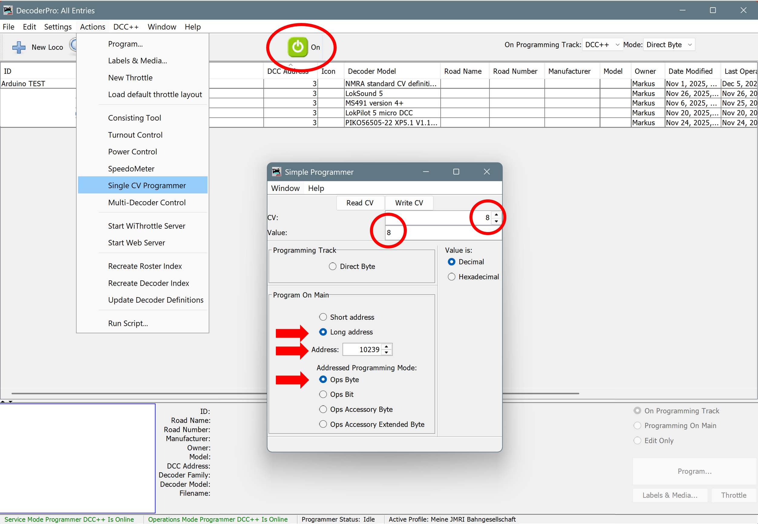
Right after flashing, the Decoder is NOT yet ready for usage, as the ATtiny's EEPROM is still on factory default and the decoder therefore has an unknown address. You can already wire up the decoder as described in the following section. Then, perform a factory reset of the decoder by writing the value 8 to CV8, using the decoder's magic address 10239. In case you forgot your decoder's address, you can always perform CV writes using the magic address 10239. If you are using DecoderPro, proceed as shown below:
Connect the LEDs as shown. Use appropriate resistors. The maximum current should be limited to 2 mA per LED. That does sound little but usually it is enough. Otherwise the LDO on the decoder gets too hot.
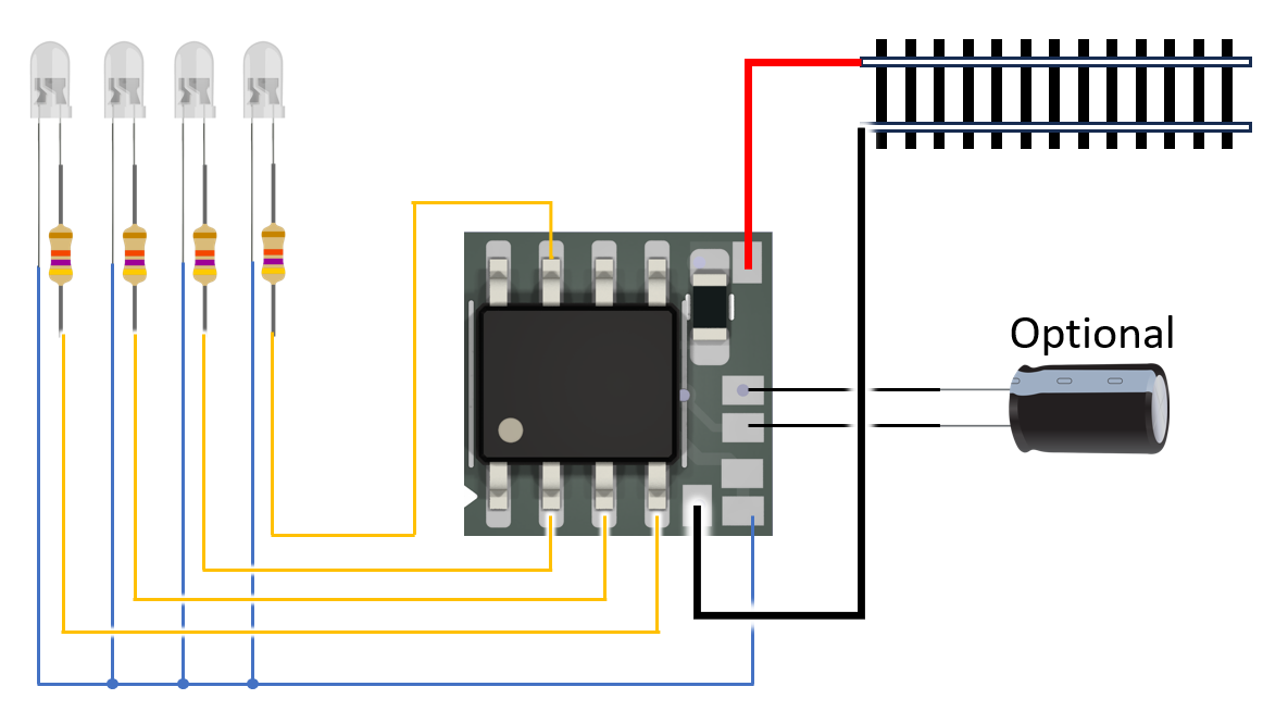
The decoder ONLY supports Programming on Main (POM) mode. It cannot generate an ACK. For CVs see the table below. The decoder will confirm each CV write with a short flash of all AUX channels.
Special note on programming the address: If you want to change the decoder's address, you must do so in the following order:
From then on, the decoder will only accept CV writes or commands to the new address. It will of course still accept commands to its consist address and it will also still be programmable via its magic address 10239.
The decoder can be reset to its default CV values by writing CV8 = 8. This is confirmed by multiple short flashes of all AUX channels.
| CV | Type | range | default Value | Description |
|---|---|---|---|---|
| 1 | address | 1...127 | 3 | short address |
| 17 | long Address high byte | 192...255 | 195 | CV17 = 192 + (address / 256) |
| 18 | long address low byte | 0...255 | 232 | CV18 = address mod 256 |
| 19 | consist address | 0...255 | 0 | consist address |
| 29 | configuration byte | 0...255 | 0 | CV29 = 0: short address; CV29 = 32: long address |
| 33 ... 54 | FunctionMap CV33: F0f CV34: F0r CV35: F1 ... CV54: F20 | 0...15 | CV35=0b00000001 (F1->AUX1) CV36=0b00000010 (F2->AUX2) CV37=0b00000100 (F3->AUX3) CV38=0b00001000 (F4->AUX4) all others = 0 | Bit0=1: Fn controls AUX1 Bit1=1: Fn controls AUX2 Bit2=1: Fn controls AUX3 Bit3=1: Fn controls AUX4 |
| 55 | forwardOnly map | 0...15 | 0 | Bit0=1: AUX1 only active when FORWARD ... Bit3=1: AUX4 only active when FORWARD |
| 56 | reverseOnly map | 0...15 | 0 | Bit0=1: AUX1 only active when REVERSE ... Bit3=1: AUX4 only active when REVERSE |
| 57 58 59 60 | Output mode AUX n | 0...2 | 0 | 0 = fade 1 = neon 2 = Blink |
| 65 66 67 68 | dimm value AUX n | 0...255 | 255 | 0 = off ... 255 = full brightness |
| 73 74 75 76 | fade speed AUX n | 0...255 | 0 | 0 = instant on/off ... 255 = very slow fading |
| 97 98 99 100 | blink on time AUX n | 0...255 | 80 | value * 10ms = on-time during blink (only active when CV57...60 = 2) |
| 105 106 107 108 | blink off time AUX n | 0...255 | 150 | value * 10ms = off-time during blink (only active when CV57...60 = 2) |
| 113 114 115 116 | speed Threshold AUX n | 0...255 | 0 | Bit7=0/1: AUX is active above/below threshold Bit0...6: speed threshold |
CV55 and CV56 (forwardOnly and reverseOnly) are evaluated for F1...F20 only. The AUX mapped to F0f/F0r are active in forward/reverse direction only, independently from forwardOnly and reverseOnly
CV113 = 0b0000000: AUX1 active for speed >= 0 (=always active)
CV114 = 0b0010000: AUX2 active for speed >= 64
CV115 = 0b1000000: AUX3 active for speed <= 0 (standstill only)
CV116 = 0b1001000: AUX4 active for speed <= 16
Copyright 2025 by Markus Grün
Software licensed under GNU General Public License v3.0, see license file in Software-folder
Hardware (Schematics, Layout, etc.) licensed under CERN-OHL-P v2 or later, see license file in Hardware-folder
THE SOFTWARE AND SOURCES ARE PROVIDED "AS IS", WITHOUT WARRANTY OF ANY KIND, EXPRESS OR IMPLIED, INCLUDING BUT NOT LIMITED TO THE WARRANTIES OF MERCHANTABILITY, FITNESS FOR A PARTICULAR PURPOSE AND NONINFRINGEMENT. IN NO EVENT SHALL THE AUTHORS OR COPYRIGHT HOLDERS BE LIABLE FOR ANY CLAIM, DAMAGES OR OTHER LIABILITY, WHETHER IN AN ACTION OF CONTRACT, TORT OR OTHERWISE, ARISING FROM, OUT OF OR IN CONNECTION WITH THE SOFTWARE OR SOURCES OR THE USE OR OTHER DEALINGS IN THE SOFTWARE OR SOURCES.
| Qty | Value | Footprint | References |
|---|---|---|---|
| 6 | Conn_01x01 | Markus:Solderpad_1x_SMD_1.0x0.7 | J1, J2, J3, J4, J5, J7 |
| 5 | TS 4148-0603 | Diode_SMD:D_0603_1608Metric_Pad1.05x0.95mm_HandSolder | D1, D2, D3, D4, D5 |
| 2 | 10u | Capacitor_SMD:C_0603_1608Metric_Pad1.08x0.95mm_HandSolder | C1, C2 |
| 1 | 100R | Resistor_SMD:R_0603_1608Metric_Pad0.98x0.95mm_HandSolder | R1 |
| 1 | 22k | Resistor_SMD:R_0603_1608Metric_Pad0.98x0.95mm_HandSolder | R2 |
| 1 | ATtiny402-SS | Package_SO:SOIC-8_3.9x4.9mm_P1.27mm | U2 |
| 1 | LM3480-5.0 | Package_TO_SOT_SMD:SOT-23 | U1 |
It measures 7.4 × 7.3 mm and has 2 copper layers, 0.6 mm thick.
17 parts, built around the ATTINY402-SSN. The full list of its parts is on this page, with links to each part's symbol and footprint where PCBKit's library has them.
From the markusgruen/DccFunctionDecoder repository on GitHub, at the commit this page was made from: the board is Hardware/DccFunctionDecoder_4ch_V1/DCC_Dekoder_Attiny402__1.kicad_pcb and its schematic Hardware/DccFunctionDecoder_4ch_V1/DCC_Dekoder_Attiny402__1.kicad_sch. PCBKit opens the board in the browser, with nothing to install.
Its repository publishes it under the GPL-3.0 licence: you may reuse it on that licence's terms (keep the author's notice, and for a copyleft licence share your changes alike).

PocketConcepts/Pocket_PSU
A variable current & voltage PSU with 3S lipo charging, balancing, and protection circuit using PPS.

k-takata/PCB_avr_dx_unbricker
UPDI High Voltage programmer for AVR Dx/Ex series

HazeCore/Nametag_Hardware
This is the hardware for out Nametag Badge for Chaos Communication Camp 2023. You can find more information about the Project at https://hazeco.re/cccamp-nametag/.


KNEAGHUST/PCB_Christmas_Tree_AGH
PCB Christmas tree designed for the AGH University of Krakow

