
2 layers34 × 76 mm

Custom ESP32-based temperature web server PCB designed in KiCad, manufactured and assembled with SMD/THT components, including LM35 sensing, USB/RS232 communication and lab validation.
Practica is an open-source printed circuit board by marcosindiano7, from the marcosindiano7/ESP32-Temperature-WebServer-PCB repository on GitHub. It is a 2-layer board of 80 × 80 mm with 73 parts on 61 nets, routed with 510 tracks and 17 vias.
It is built around the CH340N, BC547 and BC557, with the RMB2S among its other parts. Its parts include 20 resistors, 15 capacitors, 11 diodes, 4 ICs and 4 transistors.


Custom two-layer PCB designed in KiCad for an ESP32-based temperature monitoring system.
The board measures temperature using an LM35 analog sensor and allows the measured value to be monitored through a web interface served by the ESP32 module.
This project focuses on the complete hardware development flow: schematic capture, PCB layout, manufacturing files generation, board assembly and laboratory validation.
The goal of this project was to design and validate a functional printed circuit board for an IoT temperature monitoring device.
The system includes:
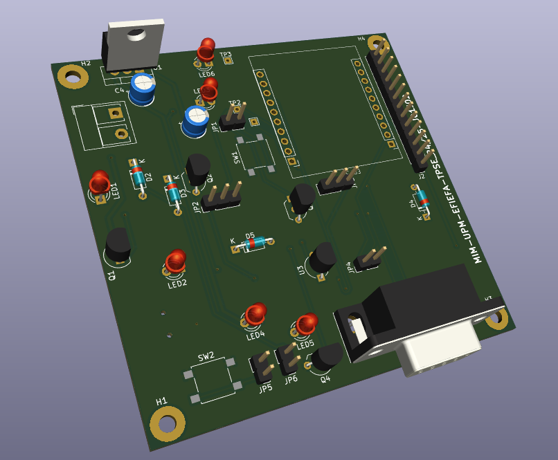
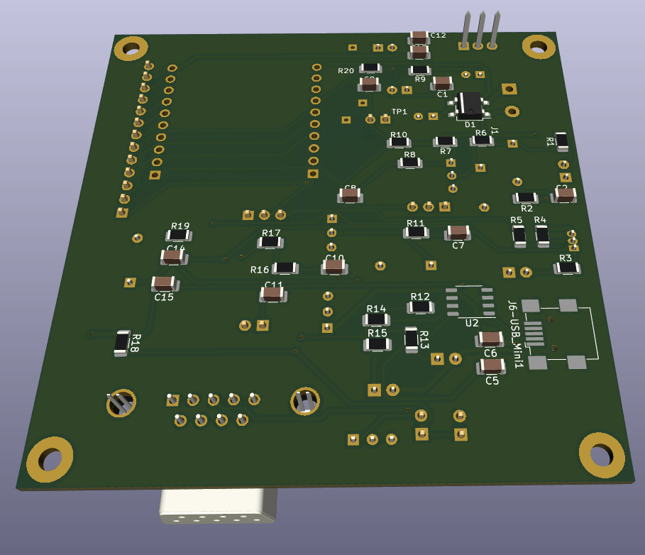
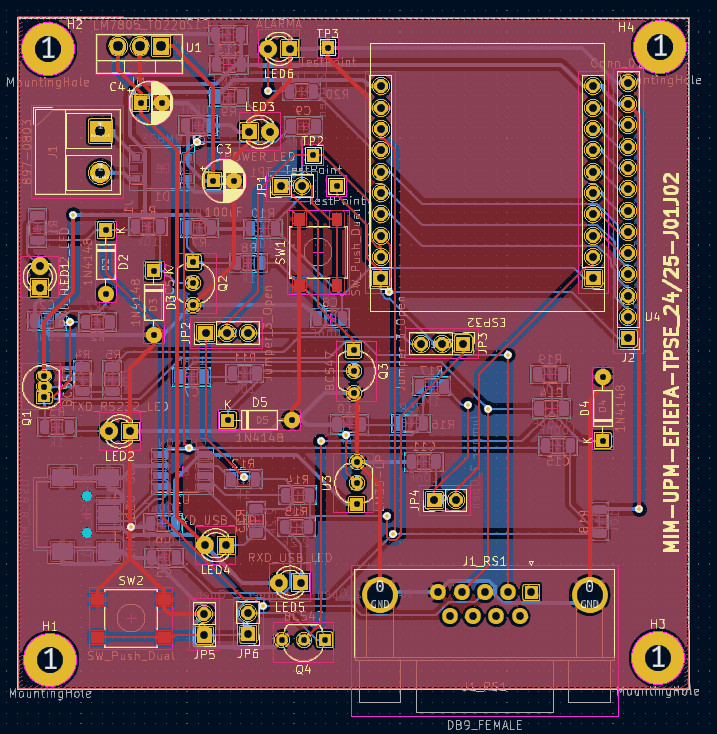


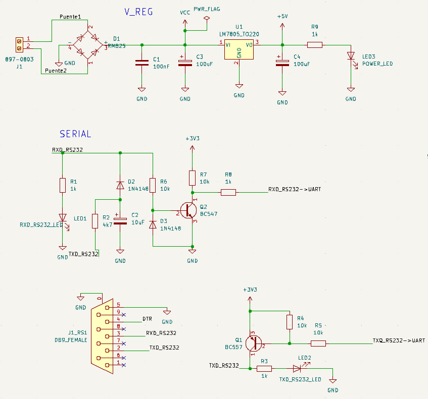
The schematic is divided into several functional blocks:
The power stage provides the regulated supply required by the system.
It includes input filtering, a linear voltage regulator and a power indicator LED.
The ESP32 module acts as the core of the system.
It is connected to the temperature sensing stage, UART communication lines, boot/reset circuitry and alarm LED.
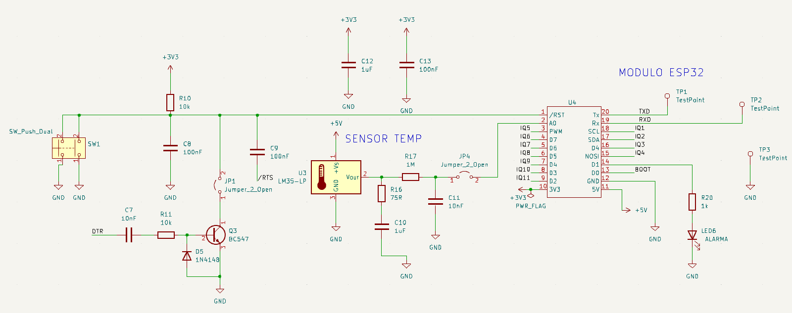
The board uses an LM35 analog temperature sensor.
Its output voltage is proportional to the measured temperature and is connected to the ESP32 analog input through a simple conditioning/filtering stage.
A CH340N USB-to-UART converter is used to provide serial communication through the USB connector.

The board also includes an RS232 communication stage with level adaptation to interface with the ESP32 UART signals.
Jumpers are used to select whether the ESP32 UART lines are connected to the USB interface or to the RS232 interface.
The design includes manual and automatic boot/reset circuitry, allowing the ESP32 to start normally or enter programming mode.
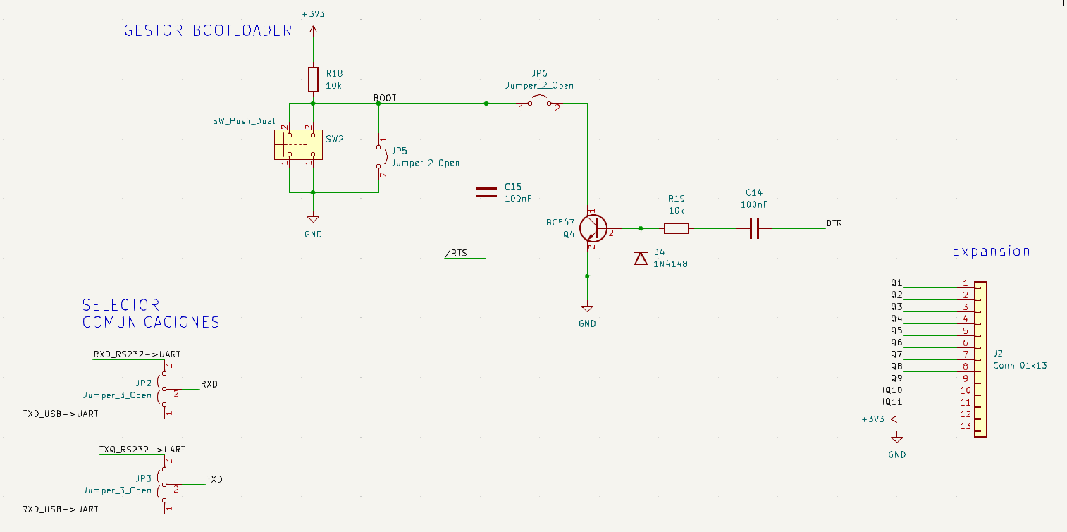
An expansion connector exposes additional ESP32 pins for future extensions or external peripherals.
.
├── hardware/
│   ├── kicad/              # KiCad project files
│   └── fabrication/        # Gerber and drill files
├── docs/
│   └── images/             # Schematic captures, PCB renders and photos
├── bom/                    # Bill of materials, if available
├── README.md
└── .gitignoreThe hardware design was developed using KiCad and includes:
The hardware/fabrication/ folder contains the production files required to manufacture the PCB:
The PCB was manufactured externally and later assembled in the laboratory.
The assembly process included both SMD and through-hole components.
Main assembled elements:
The assembled PCB was validated through several checks:
During the final test, the ESP32 web interface displayed:
Example web interface:
This repository focuses on the hardware design, PCB manufacturing files and validation process.
Firmware or software not originally developed by the author is not included.
Marcos Indiano
Electronic Communications Engineering student
Universidad Politécnica de Madrid
| Qty | Value | Footprint | References |
|---|---|---|---|
| 8 | 100nF | Capacitor_SMD:C_1206_3216Metric | C1, C5, C6, C8, C9, C13, C14, C15 |
| 8 | 10k | Resistor_SMD:R_1206_3216Metric | R4, R5, R6, R7, R10, R11, R18, R19 |
| 7 | 1k | Resistor_SMD:R_1206_3216Metric | R1, R3, R8, R9, R12, R14, R20 |
| 4 | 1N4148 | Diode_THT:D_DO-35_SOD27_P7.62mm_Horizontal | D2, D3, D4, D5 |
| 4 | Jumper_2_Open | Connector_PinHeader_2.54mm:PinHeader_1x02_P2.54mm_Vertical | JP1, JP4, JP5, JP6 |
| 4 | MountingHole | MountingHole:MountingHole_3mm_Pad | H1, H2, H3, H4 |
| 3 | BC547 | Package_TO_SOT_THT:TO-92_Inline_Wide | Q2, Q3, Q4 |
| 3 | TestPoint | TestPoint:TestPoint_THTPad_1.5x1.5mm_Drill0.7mm | TP1, TP2, TP3 |
| 2 | 100uF | Capacitor_THT:CP_Radial_D5.0mm_P2.50mm | C3, C4 |
| 2 | 10nF | Capacitor_SMD:C_1206_3216Metric | C7, C11 |
| 2 | 1uF | Capacitor_SMD:C_1206_3216Metric | C10, C12 |
| 2 | 2.2k | Resistor_SMD:R_1206_3216Metric | R13, R15 |
| 2 | Jumper_3_Open | Connector_PinHeader_2.54mm:PinHeader_1x03_P2.54mm_Vertical | JP2, JP3 |
| 2 | SW_Push_Dual | Button_Switch_SMD:SW_SPST_B3S-1000 | SW1, SW2 |
| 1 | 10uF | Capacitor_SMD:C_1206_3216Metric | C2 |
| 1 | 1M | Resistor_SMD:R_1206_3216Metric | R17 |
| 1 | 4k7 | Resistor_SMD:R_1206_3216Metric | R2 |
| 1 | 75R | Resistor_SMD:R_1206_3216Metric | R16 |
| 1 | 897-0803 | TerminalBlock_RND:TerminalBlock_RND_205-00276_1x02_P5.00mm_Vertical | J1 |
| 1 | ALARMA | LED_THT:LED_D3.0mm | LED6 |
| 1 | BC557 | Package_TO_SOT_THT:TO-92_Inline | Q1 |
| 1 | CH340N | Package_SO:SOP-8_3.9x4.9mm_P1.27mm | U2 |
| 1 | Conn_01x13 | Connector_PinHeader_2.54mm:PinHeader_1x13_P2.54mm_Vertical | J2 |
| 1 | DB9_FEMALE | Connector_Dsub:DSUB-9_Female_Horizontal_P2.77x2.84mm_EdgePinOffset4.94mm_Housed_MountingHolesOffset7.48mm | J1_RS1 |
| 1 | LM35-LP | Package_TO_SOT_THT:TO-92_Inline_Wide | U3 |
| 1 | LM7805_TO220 | Package_TO_SOT_THT:TO-220-3_Vertical | U1 |
| 1 | POWER_LED | LED_THT:LED_D3.0mm | LED3 |
| 1 | RMB2S | Package_TO_SOT_SMD:TO-269AA | D1 |
| 1 | RXD_RS232_LED | LED_THT:LED_D3.0mm | LED1 |
| 1 | RXD_USB_LED | LED_THT:LED_D3.0mm | LED5 |
| 1 | TXD_RS232_LED | LED_THT:LED_D3.0mm | LED2 |
| 1 | TXD_USB_LED | LED_THT:LED_D3.0mm | LED4 |
| 1 | USB_B_Mini | Connector_USB:USB_Mini-B_Wuerth_65100516121_Horizontal | J6-USB_Mini1 |
| 1 | ~ | Library:ESP32 | U4 |


agkaminski/ZAK181
Improved ZAK180: DIY all-in-keyboard computer featuring Z180 and floppy drive.


dotnet/iot
This repo includes .NET Core implementations for various IoT boards, chips, displays and PCBs.

robsonsmartins/usbflashprog
A memory device programmer (Flash/EPROM/E2PROM) board and software, connected to PC by USB port.

It measures 80 × 80 mm and has 2 copper layers, 1.6 mm thick.
73 parts, built around the CH340N, BC547, BC557 and RMB2S. The full list of its parts is on this page, with links to each part's symbol and footprint where PCBKit's library has them.
From the marcosindiano7/ESP32-Temperature-WebServer-PCB repository on GitHub, at the commit this page was made from: the board is hardware/KiCad/Practica.kicad_pcb and its schematic hardware/KiCad/Practica.kicad_sch. PCBKit opens the board in the browser, with nothing to install.
Its repository states no licence, so its author keeps all rights: ask marcosindiano7 before reusing the design.