

2 layers370.8 × 298.5 mm
8 Bit Computer
The-Invent0r/8-bit-Computer-PCB
These are the KiCAD files for my 8-Bit Computer.
323 parts142
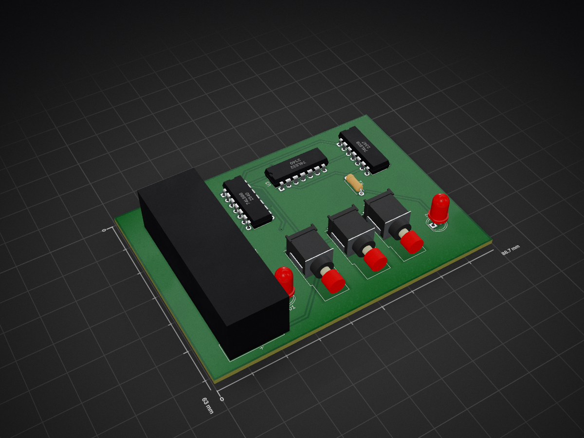
 Manideep136/Full-Adder
This project implements a Full Adder Circuit designed using KiCad. A full adder is a combinational logic circuit that performs the addition of three 1-bit binary inputs and produces two outputs: Sum and Carry.
Full Adder is an open-source printed circuit board by Manideep136, from the Manideep136/Full-Adder repository on GitHub. It is a 2-layer board of 88.7 × 63 mm with 11 parts on 33 nets, routed with 96 tracks and 5 vias.
It is built around the 74LS32SC and 74LS86. Its parts include 3 ICs, 3 switches, 2 resistors and 2 diodes.
This project implements a Full Adder Circuit designed using KiCad. A full adder is a combinational logic circuit that performs the addition of three 1-bit binary inputs and produces two outputs: Sum and Carry.
The three inputs are A, B, and Carry-in (Cin). The outputs are Sum (S) and Carry-out (Cout).
This project demonstrates the fundamentals of digital electronics, Boolean algebra, logic gates, schematic design, footprint assignment, and PCB layout.
A full adder adds three binary input bits:
It generates two outputs:
The Boolean expressions are:
Sum:
S = A XOR B XOR CinCarry-out:
Cout = (A AND B) OR (Cin AND (A XOR B))The circuit can be implemented using XOR, AND, and OR logic gates.
| A | B | Cin | Sum | Cout |
|---|---|---|---|---|
| 0 | 0 | 0 | 0 | 0 |
| 0 | 0 | 1 | 1 | 0 |
| 0 | 1 | 0 | 1 | 0 |
| 0 | 1 | 1 | 0 | 1 |
| 1 | 0 | 0 | 1 | 0 |
| 1 | 0 | 1 | 0 | 1 |
| 1 | 1 | 0 | 0 | 1 |
| 1 | 1 | 1 | 1 | 1 |
The components depend on the implementation used in the schematic.
| Component | Description | Quantity |
|---|---|---|
| 74LS86 | Quad 2-input XOR gate IC | As required |
| 74LS08 | Quad 2-input AND gate IC | As required |
| 74LS32 | Quad 2-input OR gate IC | As required |
| Push buttons or switches | Binary input controls | 3 |
| LEDs | Sum and carry indicators | 2 |
| Resistors | LED current-limiting resistors | 2 |
| Connectors | Power and input/output connections | As required |
Note: The IC quantities and connections must match the actual schematic. A 74LS86 alone is not sufficient to implement every full-adder function; AND and OR logic is also required unless an equivalent implementation is used.
For example, when A = 1, B = 1, and Cin = 1:
  1
  1
+ 1
---
 11 (binary)
Therefore, Sum = 1 and Carry-out = 1.
The PCB design process includes:
For standard 74LS-series ICs, use a regulated 5 V supply and follow the manufacturer's datasheet for input voltage limits and unused input handling.
Through this project, I learned:
KiCad 9.0
This project is intended for educational and learning purposes. You may modify and improve the design for your own digital electronics projects.
| Qty | Value | Footprint | References |
|---|---|---|---|
| 3 | SW_Push_SPDT | Button_Switch_THT:SW_NKK_BB15AH | SW1, SW2, SW3 |
| 2 | LED | LED_THT:LED_D5.0mm | D1, D2 |
| 2 | R | Resistor_THT:R_Axial_DIN0207_L6.3mm_D2.5mm_P7.62mm_Horizontal | R1, R2 |
| 1 | 74LS08 | Package_DIP:DIP-14_W7.62mm | U2 |
| 1 | 74LS32 | Package_DIP:DIP-14_W7.62mm | U3 |
| 1 | 74LS86 | Package_DIP:DIP-14_W7.62mm | U1 |
| 1 | Battery | Battery:BatteryHolder_Bulgin_BX0034_1xAAA | BT1 |
It measures 88.7 × 63 mm and has 2 copper layers, 1.6 mm thick.
11 parts, built around the 74LS32SC and 74LS86. The full list of its parts is on this page, with links to each part's symbol and footprint where PCBKit's library has them.
From the Manideep136/Full-Adder repository on GitHub, at the commit this page was made from: the board is Full Adder/Full Adder.kicad_pcb and its schematic Full Adder/Full Adder.kicad_sch. PCBKit opens the board in the browser, with nothing to install.
Its repository states no licence, so its author keeps all rights: ask Manideep136 before reusing the design.
The-Invent0r/8-bit-Computer-PCB
These are the KiCAD files for my 8-Bit Computer.

hkzlab/CGA_Redux
The Color Graphics Adapter Redux board is a more or less faithful clone of the original IBM CGA, based on the original schematics

profdc9/ISACard
A ISA card for PC/XT/AT that has SD storage and SPI/I2C interfaces using a ATMEGA328P

btb/LanguageCard
An Apple II Language Card. Based on a design by iz8dwf


fortinsylvain/MyCpu
Home brew CPU Hardware with 1-bit ALU implementation using 74LSxx, a micro-code and assembler coded in C#.

clemarfolly/Microdigital-TK2000
Reprodução da PCB do TK-2000 da Microdigital, clone do Micro-Professor MPF-II
