2 layers57 × 55.2 mm
LogicAnalyzer
gusmanb/logicanalyzer
24 channel, 100Msps logic analyzer hardware and software
10 parts5.1kGPL-3.0
 Manideep136/Echo-Debug-
The Amazon Echo Gen 3 contains a hidden USB interface that can be accessed using this adapter board. The purpose of this PCB is to provide a clean and convenient connection to the internal USB interface instead of…
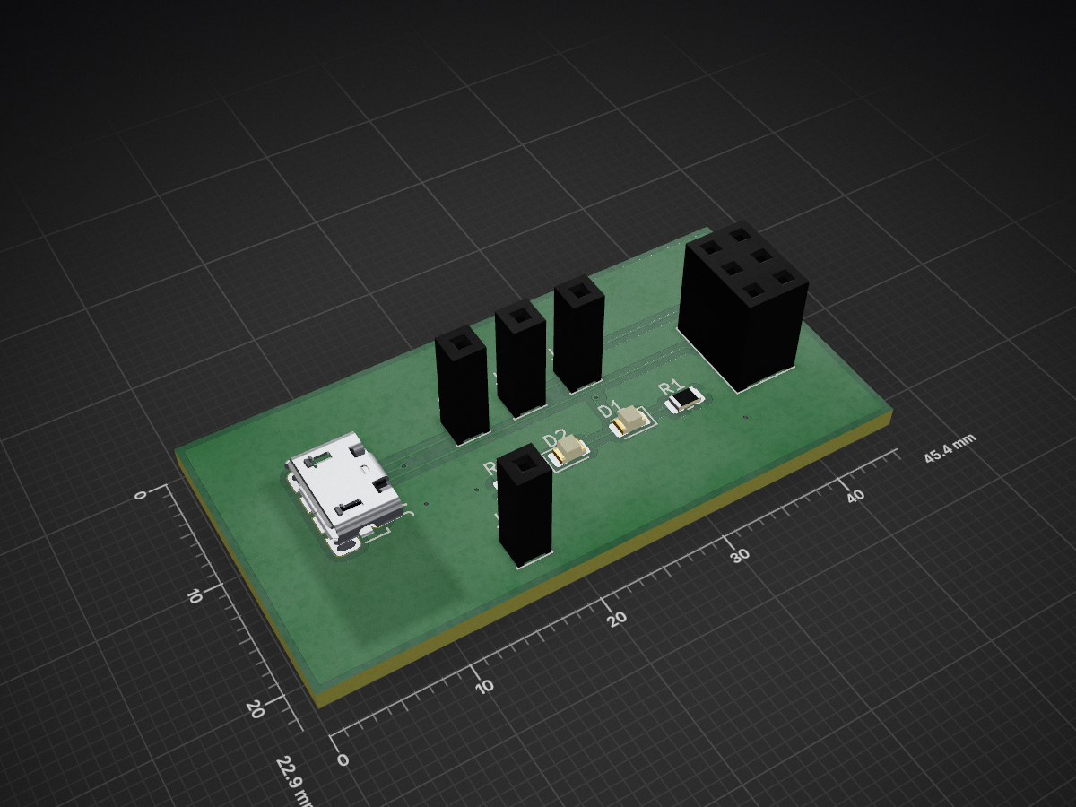
Echo Debug- is an open-source printed circuit board by Manideep136, from the Manideep136/Echo-Debug- repository on GitHub. It is a 2-layer board of 45.4 × 22.9 mm with 10 parts on 14 nets, routed with 54 tracks and 5 vias.
Its parts include 6 connectors, 2 resistors and 2 diodes.
Echo Debug Gen3
Echo Debug Gen3 is a custom adapter PCB designed for the Amazon Echo Gen 3.
The Amazon Echo Gen 3 contains a hidden USB interface that can be accessed using this adapter board. The purpose of this PCB is to provide a clean and convenient connection to the internal USB interface instead of cutting a normal USB cable and manually soldering wires.
This project was designed using KiCad and includes the complete schematic, PCB layout, Bill of Materials (BOM), and manufacturing files.
The main objectives of this project are:
The original project's v1.1 revision corrected the USB differential-pair connection, removed zero-ohm resistors, added optional LEDs for +12 V and +1.9 V, rounded the PCB corners, and changed the USB connector to a lower-cost variant. :contentReference[oaicite:1]{index=1}
│ └── Project images │ └── README.md
| Qty | Value | Footprint | References |
|---|---|---|---|
| 2 | LED | LED_SMD:LED_0805_2012Metric | D1, D2 |
| 2 | R | Resistor_SMD:R_0805_2012Metric | R1, R2 |
| 1 | 1050170001 | 1050170001:MOLEX_1050170001 | J7 |
| 1 | Echo Gen 3 | Connector_PinSocket_2.54mm:PinSocket_2x03_P2.54mm_Vertical | J2 |
| 1 | GND | Connector_PinSocket_2.54mm:PinSocket_1x01_P2.54mm_Vertical | J6 |
| 1 | V1.9 | Connector_PinSocket_2.54mm:PinSocket_1x01_P2.54mm_Vertical | J5 |
| 1 | V12 | Connector_PinSocket_2.54mm:PinSocket_1x01_P2.54mm_Vertical | J4 |
| 1 | VBUS | Connector_PinSocket_2.54mm:PinSocket_1x01_P2.54mm_Vertical | J3 |
It measures 45.4 × 22.9 mm and has 2 copper layers, 1.6 mm thick.
10 parts. The full list of its parts is on this page, with links to each part's symbol and footprint where PCBKit's library has them.
From the Manideep136/Echo-Debug- repository on GitHub, at the commit this page was made from: the board is Echo Debug/Echo Debug.kicad_pcb and its schematic Echo Debug/Echo Debug.kicad_sch. PCBKit opens the board in the browser, with nothing to install.
Its repository states no licence, so its author keeps all rights: ask Manideep136 before reusing the design.
gusmanb/logicanalyzer
24 channel, 100Msps logic analyzer hardware and software

byrantech/laptop
anyon_e, a highly integrated, high end, open source laptop. Attempt the impossible.

joeycastillo/Sensor-Watch
A board replacement for the classic Casio F-91W wristwatch


OLIMEX/OLINUXINO
OLINUXINO is Open Source / Open Hardware, low cost from EUR 24 Linux Industrial grade Single Board Computer capable to operate -25+85C

rusefi/rusefi
rusefi - GPL internal combustion engine control unit

VoronDesign/Voron-Hardware
Cool Hardware designed by the Voron Design group

hoglet67/RGBtoHDMI
Bare-metal Raspberry Pi project that provides pixel-perfect sampling of Retro Computer RGB/YUV video and conversion to HDMI