
2 layers57 × 55.2 mm
LogicAnalyzer
gusmanb/logicanalyzer
24 channel, 100Msps logic analyzer hardware and software
10 parts5.1kGPL-3.0

LT3080 adjustable LDO KiCad PCB design
LDO is an open-source printed circuit board by macnamtran, from the macnamtran/LDO repository on GitHub. It is a 2-layer board of 28.9 × 13.4 mm with 10 parts on 6 nets, routed with 37 tracks and 4 vias.
Its parts include 4 capacitors, 2 resistors, 2 connectors and 1 IC.
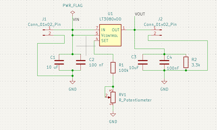
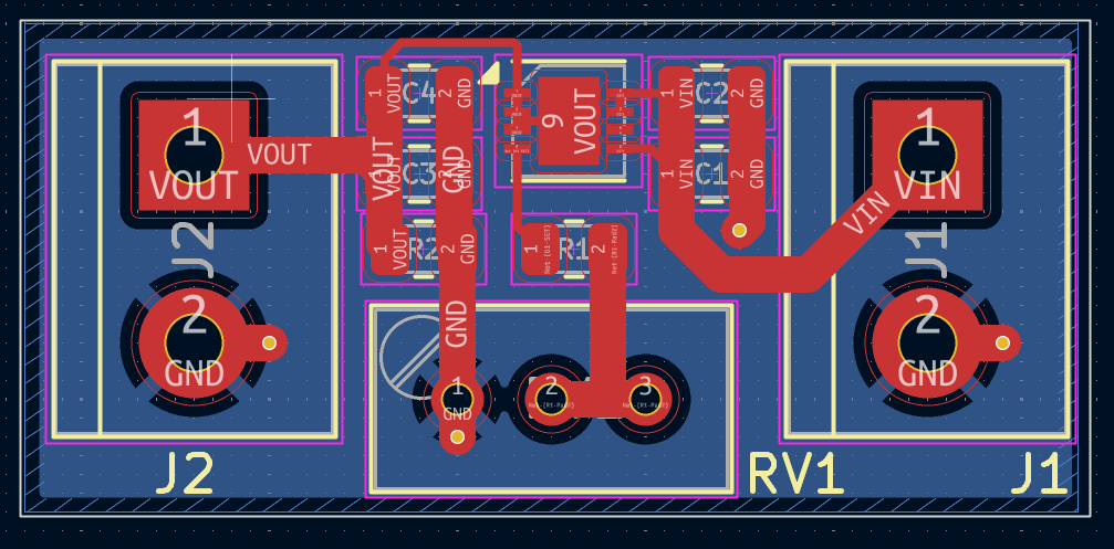
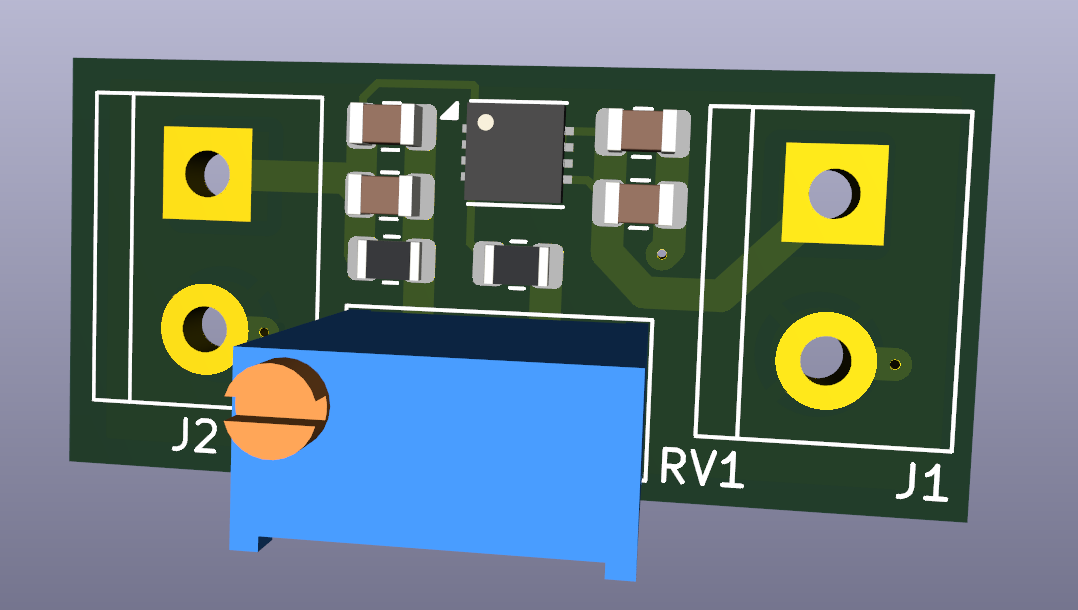
This project is a KiCad PCB design for an adjustable low-dropout linear regulator board using the LT3080xDD. The board takes a DC input voltage and produces an adjustable regulated output voltage.
The purpose of this design is to understand:
| Parameter | Value |
|---|---|
| Regulator IC | LT3080xDD |
| PCB tool | KiCad 9 |
| Input voltage | VIN, nominal 1-5 V |
| Output voltage | Adjustable |
| Target output current | Approximately 0.3 A to 0.5 A |
| PCB type | 2-layer PCB |
| Main ground strategy | Bottom-layer GND plane |
The LT3080xDD package has multiple pins connected to the same electrical nets.
| LT3080 Pin | Function | PCB Connection |
|---|---|---|
| Pins 1, 2, 3 | OUT | Connected to VOUT |
| Pin 4 | SET | Connected to R1/RV1 voltage-setting network |
| Pin 5 | VCONTROL | Connected to VIN |
| Pin 6 | NC | Not connected |
| Pins 7, 8 | IN | Connected to VIN |
| Pad 9 | OUT exposed pad | Connected to VOUT, not GND |
Important layout note: the exposed pad, pad 9, is VOUT, not ground. It should connect to the VOUT copper area and should not be connected to the GND plane.
The LT3080 uses a SET pin current to define the output voltage. According to the datasheet, the SET pin current is approximately:
From the datasheet:
a. Stable with 2.2uF ceramic output capacitor, ESR <= 0.5 OHM ==> Connect VIN and VOUT with 2 capacitor: 10uF for stability requirement, 100nF for extra bypassing for fast signal
b. VOUT = RSET * 10uA, VOUT = [1V, 5V] => RSET = [100kOHM, 500kOHM] => RSET = 100kOHM, RV1 = 390kOHM
c. Min load current = 0.5mA R2_max = VOUT_min/ILoad_min=1V/0.5mA = 2kOHM R2_min = VOUT_max/Iwaste_max = 5V/5mA = 1kOHM ==> Pick R2 = 1kOHM
Basic rules used in this PCB: - high current path -> wider trace - low current signal/control path -> thinner trace - ground return path -> copper plane
For this LT3080 LDO board, the important current paths are: VIN path: J1 VIN -> input capacitors -> LT3080 IN/VCONTROL
VOUT path: LT3080 OUT/pad 9 -> output capacitors/R2 -> J2 VOUT
GND path: load/capacitor-return current -> GND plane
Route width summary: - VIN/VOUT main trace: 1.0mm - short necks into LT3080 small pins/pin connections: 0.25mm
| Qty | Value | Footprint | References |
|---|---|---|---|
| 2 | Conn_01x02_Pin | TerminalBlock:TerminalBlock_bornier-2_P5.08mm | J1, J2 |
| 1 | 10 uF | Capacitor_SMD:C_0805_2012Metric | C1 |
| 1 | 100 nF | Capacitor_SMD:C_0805_2012Metric | C2 |
| 1 | 100k | Resistor_SMD:R_0805_2012Metric | R1 |
| 1 | 100nF | Capacitor_SMD:C_0805_2012Metric | C4 |
| 1 | 10uF | Capacitor_SMD:C_0805_2012Metric | C3 |
| 1 | 3.3k | Resistor_SMD:R_0805_2012Metric | R2 |
| 1 | LT3080xDD | Package_DFN_QFN:DFN-8-1EP_3x3mm_P0.5mm_EP1.66x2.38mm | U1 |
| 1 | R_Potentiometer | Potentiometer_THT:Potentiometer_Bourns_3296W_Vertical | RV1 |
It measures 28.9 × 13.4 mm and has 2 copper layers, 1.6 mm thick.
10 parts. The full list of its parts is on this page, with links to each part's symbol and footprint where PCBKit's library has them.
From the macnamtran/LDO repository on GitHub, at the commit this page was made from: the board is LDO.kicad_pcb and its schematic LDO.kicad_sch. PCBKit opens the board in the browser, with nothing to install.
Its repository states no licence, so its author keeps all rights: ask macnamtran before reusing the design.
gusmanb/logicanalyzer
24 channel, 100Msps logic analyzer hardware and software

byrantech/laptop
anyon_e, a highly integrated, high end, open source laptop. Attempt the impossible.

joeycastillo/Sensor-Watch
A board replacement for the classic Casio F-91W wristwatch


OLIMEX/OLINUXINO
OLINUXINO is Open Source / Open Hardware, low cost from EUR 24 Linux Industrial grade Single Board Computer capable to operate -25+85C

rusefi/rusefi
rusefi - GPL internal combustion engine control unit

VoronDesign/Voron-Hardware
Cool Hardware designed by the Voron Design group

hoglet67/RGBtoHDMI
Bare-metal Raspberry Pi project that provides pixel-perfect sampling of Retro Computer RGB/YUV video and conversion to HDMI