2 layers148.6 × 192.2 mm
Badge
NuttyShell/NuttyBadge
NuttyBadge: A NuttyShell crafted multi-tool. Opensourced Hardawre and Software
169 parts31GPL-3.0

 M7md0010/ESP32-S3-TBone
Custom T-bone form-factor ESP32-S3 development board for breadboard-friendly prototyping
ESP32-S3-TBone is an open-source printed circuit board by M7md0010, from the M7md0010/ESP32-S3-TBone repository on GitHub. It is a 4-layer board of 93.6 × 51.7 mm with 59 parts on 71 nets, routed with 1,052 tracks and 168 vias.
It is built around the ESP32-S3-WROOM-1-N8, CH343P and AMS1117-3.3, with the SS34, MMBT3904 and WS2812B among its other parts. Its parts include 15 resistors, 13 connectors, 10 capacitors, 8 diodes and 5 switches. It belongs with the microcontroller boards boards and the ESP32 boards of this library.


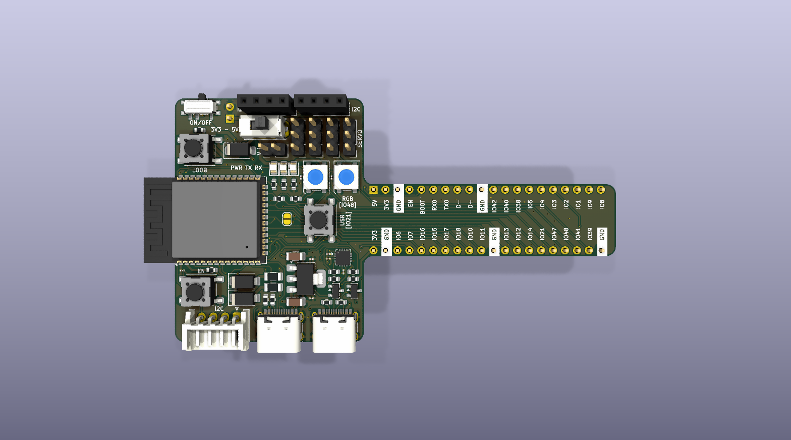
Custom T-bone form-factor ESP32-S3 development board engineered to resolve solderless breadboard real estate constraints by exposing dual-sided tie points.




The ESP32-S3-TBone is a purpose-engineered development board built around the ESP32-S3-WROOM-1 module. Unlike standard rectangular devkits that monopolize the entire breadboard, the T-bone form factor features a narrowed neck section that straddles the center channel while the head section extends beyond the breadboard edge — freeing up both sides of the breadboard for prototyping access to all GPIO tie points.
| Parameter | Specification |
|---|---|
| Core | Xtensa® dual-core 32-bit LX7 |
| Clock | Up to 240 MHz |
| Flash | 16 MB (Quad SPI) |
| SRAM | 512 KB |
| Connectivity | Wi-Fi 802.11 b/g/n + Bluetooth 5 (LE) |
| USB | Native USB 2.0 OTG + UART via CH343P |
| GPIO | Fully broken-out via dual header rows |
┌─────────────────────────────────────────────────────────┐
│  Layer 1 — F.Cu (Top)                                   │
│  → High-density signal routing, component pads,         │
│    USB differential pairs, crystal oscillator traces     │
├─────────────────────────────────────────────────────────┤
│  Layer 2 — In1.Cu (Inner 1)                             │
│  → Solid continuous ground (GND) reference plane        │
│    Provides low-impedance return path for all signals   │
├─────────────────────────────────────────────────────────┤
│  Layer 3 — In2.Cu (Inner 2)                             │
│  → Partitioned low-impedance power planes               │
│    • 3V3 polygon pour — main logic supply               │
│    • 5V rail — USB VBUS passthrough                     │
│    • VBUS — upstream USB input power                    │
├─────────────────────────────────────────────────────────┤
│  Layer 4 — B.Cu (Bottom)                                │
│  → Bottom interconnects, ground return stitching,       │
│    thermal relief pads, and auxiliary signal routing     │
└─────────────────────────────────────────────────────────┘A continuous array of stitching vias along the board perimeter connects the top and bottom ground pours, forming a Faraday cage effect. This:
The interior corners at the T-bone neck-to-head transition use chamfered/radiused fillets to accommodate standard CNC routing bit diameters (≥ 0.8 mm). Sharp 90° interior corners are physically impossible to mill and would cause fabrication rejects.
The --subtract-soldermask flag was used during Gerber generation to automatically clip silkscreen artwork wherever it overlaps exposed copper pads. This prevents:
Both USB-C ports implement the correct CC1/CC2 pull-down resistor network (5.1 kΩ to GND) on each Configuration Channel pin, advertising the device as a UFP (Upstream Facing Port) sink per USB Type-C spec Rev 2.0. This ensures reliable cable detection and power negotiation with all USB-C hosts and chargers.
The board outline (exported as .step from KiCad) was imported into Autodesk Fusion 360 alongside a reference breadboard CAD model to perform:
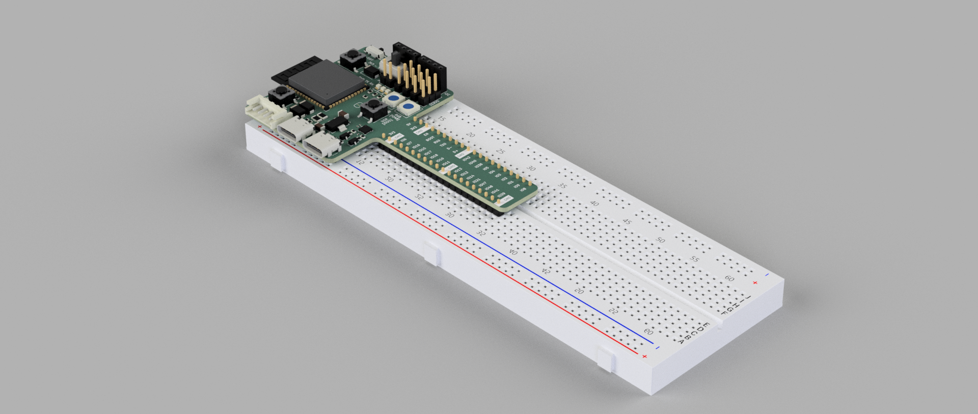
| Front (3D Render) | Back (3D Render) |
|---|---|
| 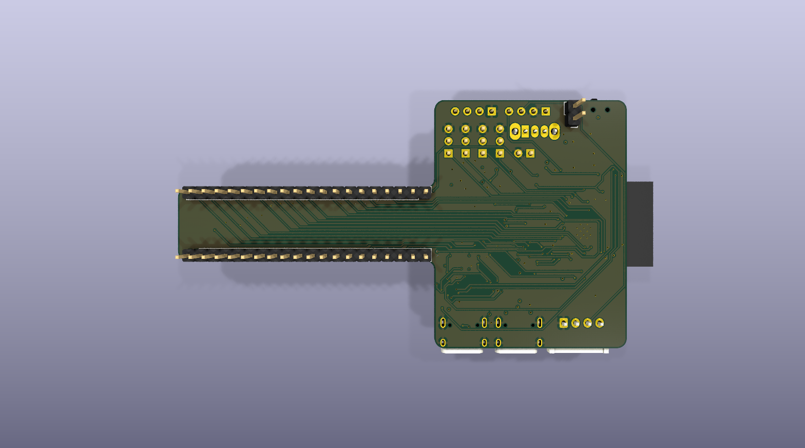 |
| Front (No Components) | Back (No Components) |
|---|---|
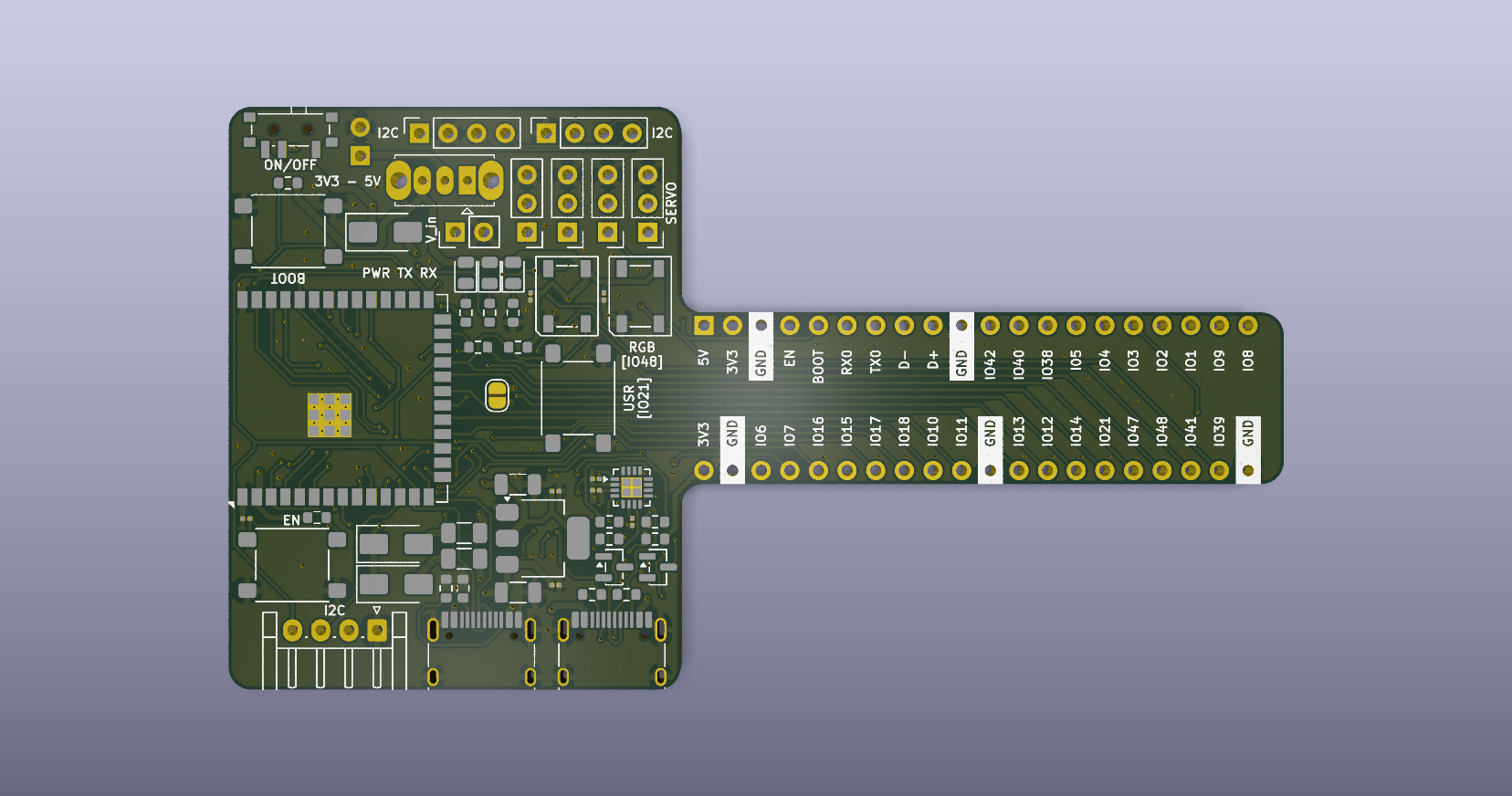 | 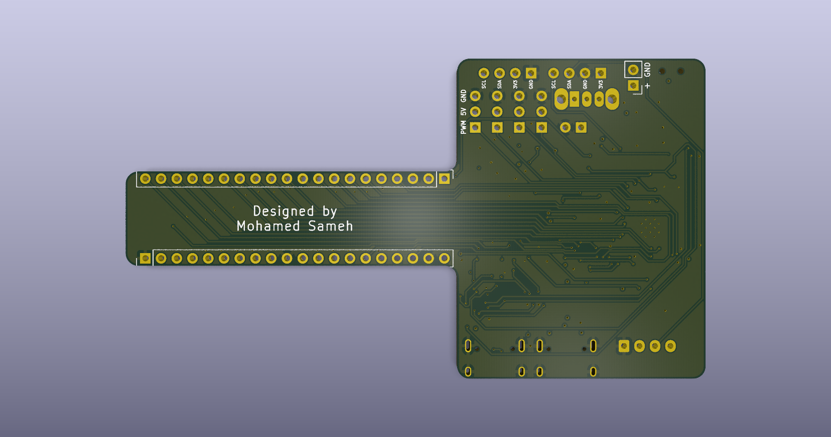 |
ESP32-S3-TBone/
├── hardware/
│   ├── schematics/
│   │   ├── schematic.pdf            # Exported schematic drawing (PDF)
│   │   └── v1.0.kicad_sch           # KiCad schematic source
│   ├── pcb/
│   │   ├── v1.0.kicad_pcb           # KiCad PCB layout source
│   │   ├── v1.0.kicad_pro           # KiCad project file
│   │   └── v1.0.kicad_dru           # KiCad design rules
│   ├── gerbers/
│   │   ├── gerbers.zip              # Production-ready Gerber + Drill archive
│   │   ├── v1.0-F_Cu.gtl            # Front copper
│   │   ├── v1.0-In1_Cu.g1           # Inner layer 1 (GND plane)
│   │   ├── v1.0-In2_Cu.g2           # Inner layer 2 (Power planes)
│   │   ├── v1.0-B_Cu.gbl            # Back copper
│   │   ├── v1.0-F_Mask.gts          # Front solder mask
│   │   ├── v1.0-B_Mask.gbs          # Back solder mask
│   │   ├── v1.0-F_Silkscreen.gto    # Front silkscreen
│   │   ├── v1.0-B_Silkscreen.gbo    # Back silkscreen
│   │   ├── v1.0-Edge_Cuts.gm1       # Board outline
│   │   ├── v1.0.drl                 # Excellon drill file
│   │   ├── v1.0-drl_map.gbr         # Drill map (Gerber X2)
│   │   └── ...                      # Additional fabrication layers
│ └── mechanical/If you modify the KiCad source files, regenerate all outputs using kicad-cli:
# Gerber layers (with soldermask-clipped silkscreen)
kicad-cli pcb export gerbers --subtract-soldermask \
  -o hardware/gerbers/ hardware/pcb/v1.0.kicad_pcb

# Excellon drill files + Gerber X2 drill map
kicad-cli pcb export drill --generate-map --map-format gerberx2 \
  -o hardware/gerbers/ hardware/pcb/v1.0.kicad_pcb

# Schematic PDF
kicad-cli sch export pdf \
  -o hardware/schematics/schematic.pdf hardware/schematics/v1.0.kicad_sch

# STEP 3D assembly (skip DNP, substitute models)
kicad-cli pcb export step --no-dnp --subst-models \
-o hardware/mechanical/ESP32-S3-TBone.step hardware/pcb/v1.0.kicad_pcbThis project is licensed under the MIT License — see the LICENSE file for details.
Designed & engineered by @M7md0010
| Qty | Value | Footprint | References |
|---|---|---|---|
| 7 | 10kΩ | Resistor_SMD:R_0603_1608Metric | R3, R4, R5, R8, R9, R10, R11 |
| 6 | 100 nF | Capacitor_SMD:C_0201_0603Metric | C1, C2, C3, C4, C5, C6 |
| 4 | 5.1kΩ | Resistor_SMD:R_0603_1608Metric | R1, R2, R6, R7 |
| 4 | Conn_01x03_Pin | Connector_PinHeader_2.54mm:PinHeader_1x03_P2.54mm_Vertical | J3, J4, J5, J6 |
| 3 | 1kΩ | Resistor_SMD:R_0603_1608Metric | R13, R14, R15 |
| 3 | LED | LED_SMD:LED_0805_2012Metric | D6, D7, D8 |
| 3 | SS34 | Diode_SMD:D_SMA | D1, D2, D3 |
| 3 | SW_Push | Button_Switch_SMD:SW_SPST_PTS645Sx43SMTR92 | SW1, SW2, SW3 |
| 2 | 100nF | Capacitor_SMD:C_0201_0603Metric | C8, C9 |
| 2 | 22μF | Capacitor_SMD:C_1206_3216Metric | C7, C10 |
| 2 | Conn_01x02_Pin | Connector_PinHeader_2.54mm:PinHeader_1x02_P2.54mm_Vertical | J14, J15 |
| 2 | Conn_01x04_Pin | Connector_PinSocket_2.54mm:PinSocket_1x04_P2.54mm_Vertical | J1, J2 |
| 2 | Conn_01x20_Pin | Connector_PinHeader_2.54mm:PinHeader_1x20_P2.54mm_Vertical | J8, J9 |
| 2 | MMBT3904 | Package_TO_SOT_SMD:SOT-23 | Q1, Q2 |
| 2 | Thermistor_PTC | Fuse:Fuse_1206_3216Metric | TH1, TH2 |
| 2 | USB_C_Receptacle_USB2.0_14P | Connector_USB:USB_C_Receptacle_HRO_TYPE-C-31-M-12 | J7, J11 |
| 2 | WS2812B | LED_SMD:LED_WS2812B_PLCC4_5.0x5.0mm_P3.2mm | D9, D10 |
| 1 | 330Ω | Resistor_SMD:R_0603_1608Metric | R12 |
| 1 | AMS1117-3.3 | Package_TO_SOT_SMD:SOT-223-3_TabPin2 | U3 |
| 1 | CH343P | Package_DFN_QFN:WCH_QFN-16-1EP_3x3mm_P0.5mm_EP1.8x1.8mm | U1 |
| 1 | Conn_01x04_Socket | Connector_JST:JST_EH_S4B-EH_1x04_P2.50mm_Horizontal | J10 |
| 1 | ESP32-S3-WROOM-1 | RF_Module:ESP32-S3-WROOM-1 | U2 |
| 1 | Jumper_2_Open | Jumper:SolderJumper-2_P1.3mm_Open_RoundedPad1.0x1.5mm | JP2 |
| 1 | SW_SPDT | Button_Switch_SMD:SW_SPDT_PCM12 | SW4 |
| 1 | SW_SPDT | Button_Switch_THT:SW_Slide_SPDT_Straight_CK_OS102011MS2Q | SW5 |
NuttyShell/NuttyBadge
NuttyBadge: A NuttyShell crafted multi-tool. Opensourced Hardawre and Software

laminarforge/laminarforge-cad
Parametric CAD models (Rust + vcad) for LaminarForge open-source LAMP diagnostics device


aditgoyal5/Forward_Ignition_PCB
This repository is about a printed circuit board I built for Team Sammard.


It measures 93.6 × 51.7 mm and has 4 copper layers, 1.6 mm thick.
59 parts, built around the ESP32-S3-WROOM-1-N8, CH343P, AMS1117-3.3 and SS34. The full list of its parts is on this page, with links to each part's symbol and footprint where PCBKit's library has them.
From the M7md0010/ESP32-S3-TBone repository on GitHub, at the commit this page was made from: the board is hardware/pcb/v1.0.kicad_pcb and its schematic hardware/schematics/v1.0.kicad_sch. PCBKit opens the board in the browser, with nothing to install.
Its repository states no licence, so its author keeps all rights: ask M7md0010 before reusing the design.